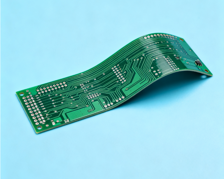
Special PCB
The 0.2mm - thick rigid PCB (while the thickness of conventional PCBs is mostly 0.8 - 1.6mm), due to its "ultra - thin and lightweight" characteristics, has become the core carrier for smart wearables, micro - sensors, and minimally - invasive medical devices. Its manufacturing process needs to overcome three pain points: "brittle base material, processing deformation, and out - of - control precision", achieving micron - level manufacturing control through a customized process
Get a Quote
I. Core Process Characteristics: Customized Processes for Ultra - thin Base Materials
The 0.2mm rigid PCB is based on an ultra - thin FR - 4 base material (core - board thickness of 0.1 - 0.12mm, paired with a 0.03 - 0.05mm prepreg) and an additional 1/3OZ (about 12μm) ultra - thin copper foil. The manufacturing process optimizes 5 key aspects based on the conventional PCB process:
- Base - material Pretreatment: Ensuring Against Deformation at the Bottom
- Material Selection and Adaptation: Select a high - rigidity ultra - thin FR - 4 base material (Tg≥160℃, flexural strength≥450MPa) to avoid brittle fracture during processing. Choose "low - profile electrolytic copper foil" (roughness Ra≤0.8μm) to reduce the stress difference between the base material and the copper foil.
- Cutting Protection: Adopt the "laser cutting + edge grinding" process. Control the laser power at 5W (to avoid high - temperature ablation of the base material). After cutting, grind the edges with 1000# sandpaper (burrs≤3μm) to prevent the base material from cracking in subsequent processes.
- Pre - baking and Shaping: Bake with hot air at 120℃ for 1.5 hours, flipping the substrate every 30 minutes to ensure the water content of the base material is ≤0.03%, reducing warping after lamination (the warpage needs to be controlled within 0.5%).
- Inner - layer Circuit Manufacturing: Micron - level Precision Control
- Thin - coating Process for Photosensitive Film: The thickness of the photosensitive film for conventional PCBs is 15 - 20μm, but for the 0.2mm rigid board, it needs to be reduced to 8 - 10μm. Use the "roll - coating + vacuum adsorption" method to avoid blurring of the circuit edges due to an overly thick film layer. Use LDI laser imaging for exposure (resolution of 5μm) with a positioning accuracy of ±1μm to meet the demand for fine - line widths of 0.08 - 0.1mm.
- Low - temperature and Slow Etching: Reduce the etchant temperature to 38±1℃ (conventional 45℃) and control the etching rate at 0.8μm/min (conventional 1.2μm/min). Etch in three times (clean after each etching) to compress the under - etching amount from 12μm to 5μm, ensuring the line - width deviation is ≤±3μm.
- Double AOI Inspection: In addition to the conventional circuit defect inspection, add "base - material deformation detection". Determine whether there are local protrusions on the substrate (protrusion height≤2μm) through optical scanning to avoid misalignment in subsequent lamination.
- Lamination: Precise Pressing of the Ultra - thin Structure
- Light - weight Lamination Design: Adopt a two - layer structure of "1 ultra - thin core board + 1 prepreg + 1 copper foil" (0.2mm boards are mostly 2 - 4 layers). Select a "low - resin - flow type" prepreg (resin - flow amount≤20%) to avoid exceeding the board - thickness standard due to excessive glue.
- Low - pressure Step - by - step Lamination: Reduce the lamination pressure from the conventional 25kg/cm² to 15 - 18kg/cm². Optimize the temperature - control curve as follows: 60℃ (10min, for exhaust) → 120℃ (20min, for initial curing) → 160℃ (30min, for complete curing), with a heating rate of ≤5℃/min at each stage to reduce thermal deformation of the base material.
- Real - time Board - thickness Monitoring: During lamination, use a "pressure sensor + thickness probe" to monitor the board thickness in real - time (the deviation needs to be ≤±0.01mm). Adjust the pressure parameters immediately if the deviation exceeds the standard to avoid batch rejection.
- Drilling and Via Metallization: Preventing Breakthrough and Ensuring Conductivity
- Micro - drill Selection and Parameter Control: Use a "tungsten - steel micro - drill" (diameter of 0.1 - 0.2mm), increase the rotation speed to 120000r/min, and reduce the feed rate to 5mm/min. Replace the drill bit every 500 holes to prevent hole - position deviation caused by drill - bit wear (hole - position deviation≤±0.02mm). After drilling, blow out the residue in the holes with 0.1MPa compressed air to avoid hole blockage.
- Low - temperature Copper - deposition Process: Control the temperature of the copper - deposition solution at 28±1℃ (conventional 35℃) and extend the copper - deposition time to 15 minutes to ensure the copper - layer thickness on the hole wall reaches 0.8 - 1μm (conventional 0.5μm). After copper - deposition, add a "hole - conductivity test". Use a micro - current detector (10mA current) to check for open - circuits in the holes, and the qualification rate needs to reach 100%.
- Thin - copper Electro - plating Reinforcement: Reduce the electro - plating current density from 1.5A/dm² to 1A/dm² and control the electro - plating time at 20 minutes to thicken the copper layer on the hole wall to 5 - 8μm, avoiding substrate deformation caused by over - electro - plating.
- Post - treatment: Preventing Damage and Ensuring Reliability
- Thin - coating and Curing of Solder - mask Layer: Reduce the thickness of the solder - mask ink from 20 - 30μm to 10 - 15μm. Use the "screen - printing + vacuum defoaming" process to avoid exceeding the board - thickness standard due to ink accumulation. Reduce the curing temperature to 140℃ for 60 minutes (conventional 150℃) to reduce substrate warping caused by thermal stress.
- Surface - treatment Adaptation: Give priority to "tin - plating" or "OSP" surface treatment (thickness≤3μm) to avoid increasing the board thickness with the gold - plating process (gold - layer + nickel - layer thickness≥7μm). After treatment, use a "micro - force test pen" to check the surface adhesion (adhesion≥4B) to prevent coating peeling.
- Protection in Shape Processing: Adopt the "laser cutting + fixture fixation" process. Set the laser power at 3W (to avoid high - temperature damage). Protect the edge of the substrate with 0.05MPa inert gas (nitrogen) during cutting to prevent delamination after cutting. After cutting, conduct a full inspection with a "thickness gauge" to ensure the board - thickness uniformity (the thickness difference on the same board≤0.02mm).
II. Core Process Difficulties and Breakthrough Solutions
- Brittle Fracture of the Base Material during Processing
- Pain Point: The thickness of the 0.2mm base material is only 1/8 of that of a conventional board. During mechanical processing (such as cutting and drilling), "edge chipping" is likely to occur (a chipping length of ≥0.5mm means rejection), and the rejection rate in the initial trial production can reach 15%.
- Solution: ① Use a "vacuum - adsorption fixture" (adsorption force of 0.3MPa) throughout the processing to avoid substrate deformation caused by mechanical clamping pressure. ② Immediately coat the edges with "epoxy resin edge - sealing liquid" (thickness of 5μm) after cutting/drilling to enhance crack resistance. ③ Store the base material in a "hard tray with layered placement" to avoid stacking and extrusion.
- Excessive Board - thickness Deviation after Lamination
- Pain Point: It is difficult to control the resin - flow amount of the ultra - thin prepreg. The board - thickness deviation after lamination easily exceeds ±0.03mm (the design requirement is ±0.02mm), affecting subsequent component mounting.
- Solution: ① "Pre - press and shape" the prepreg in advance (100℃/5kg/cm², 10min) to reduce the resin - flow fluctuation during lamination. ② Install "thickness - limiting blocks" (accuracy of ±0.005mm) inside the lamination mold to forcibly control the board thickness. ③ After laminating the first piece of each batch, scan the whole board with a "laser thickness gauge" (accuracy of 0.001mm). Start mass production only after it is qualified.
- Low Precision of Circuit Etching
- Pain Point: The ultra - thin copper foil (12μm) is prone to "over - etching" during etching, causing the 0.1mm line width to shrink to less than 0.08mm, exceeding the design tolerance.
- Solution: ① Use a "negative - type photosensitive film" (with 30% higher etching resistance than the conventional positive - type film) to reduce the erosion of the etchant on the circuit edges. ② Add "line - width compensation electro - plating" after etching. Electro - plate with a current of 1A/dm² for 3 minutes to bring the line - width deviation back within ±3μm. ③ Establish an "etching parameter database" to automatically match the etching time according to the base - material thickness and copper - foil specifications (error≤10 seconds).
III. Application Scenarios and Process - adaptation Cases
- Smart Wearable Devices: For example, the motherboard of a Huawei watch (0.2mm 4 - layer PCB) adopts the "laser cutting + LDI exposure" process to achieve a 0.08mm fine - line width. At the same time, "tin - plating surface treatment" is used to reduce the board thickness, meeting the mini - assembly requirements of the watch.
- Minimally - invasive Medical Sensors: The 0.2mm PCB for a blood - glucose monitoring sensor needs to be processed in a sterile environment. Add "plasma cleaning" (to remove surface impurities) and "vacuum packaging" in the process to ensure biocompatibility. At the same time, use "low - temperature lamination" to avoid the release of harmful substances from the base material.


