PCB developing line
In the pattern - transfer process of PCB manufacturing, the Developing Line is a core device bridging "exposure" and "etching". Its key function is to remove the unexposed photoresist (Dry Film or Liquid Photoresist) on the PCB substrate through chemical reactions. This reveals the circuit patterns concealed within the photoresist after exposure, providing a clear and precise "protection template" for the subsequent etching process. If the exposed PCB is likened to an "undeveloped film", the Developing Line is the crucial step for "image revelation", directly determining the accuracy of PCB circuit patterns, edge integrity, and production yield.
Get a Quote
I. Core Working Principle: Synergy of Chemical Dissolution and Physical Assistance
The essence of PCB developing is selective chemical dissolution. Leveraging the photochemical properties of photoresist (it cross - links and solidifies after exposure and is insoluble in the developer; the unexposed part remains in a linear structure and is soluble in the developer), through the chemical reaction between the developer and the unexposed photoresist, the photoresist in non - circuit areas is removed, while the solidified photoresist in circuit areas is retained. Its core principle can be broken down into three key steps:
- Pre - Wetting: Reducing the Surface Tension of the Developer
Before developing, the PCB first enters the pre - wet tank and comes into contact with deionized water (DI Water) through spraying or immersion. The core functions of this step are:
- Wetting the PCB surface, especially in tiny areas such as hole walls and circuit gaps, reducing the surface tension of the developer, and preventing "droplet residues" or "area omissions" of the developer on the substrate surface.
- Initially cleaning dust on the substrate surface and small photoresist debris remaining after exposure, preventing "dot - like defects" after developing.
- Balancing the substrate temperature (usually controlled at 25 - 30°C) to avoid uneven developing rates caused by a large temperature difference between the subsequent developer and the substrate.
- Developing: Selectively Dissolving Unexposed Photoresist
The pre - wet PCB then enters the developing tank, which is the core process of the developing line. The key lies in "precisely controlling the chemical dissolution process", and the core mechanisms are as follows:
- Developer Selection: Match the developer according to the type of photoresist (positive or negative photoresist). In PCB manufacturing, over 90% use positive photoresist (solidifies after exposure and is soluble when unexposed), and the corresponding developer is mostly a weakly alkaline solution (such as a 1 - 2% sodium carbonate Na₂CO₃ solution, a 1.5 - 2.5% sodium bicarbonate NaHCO₃ solution). If negative photoresist (solidifies when unexposed and is soluble when exposed) is used, an organic solvent - based developer (such as xylene, cyclohexanone) is required, but it has been gradually phased out due to poor environmental friendliness.
- Dissolution Reaction: The unexposed positive photoresist (linear polymer structure) undergoes a "saponification reaction" with the alkaline developer, generating carboxylates that are soluble in water and are carried away with the flow of the developer. The photoresist after exposure undergoes cross - linking polymerization due to ultraviolet irradiation (forming a three - dimensional network structure) and cannot react with the developer, thus being completely retained to form a circuit pattern consistent with the design.
- Process Parameter Control: The key to the developing effect lies in "three elements":
- Temperature: The temperature of the developer is usually controlled at 30 - 35°C (for every 1°C increase in temperature, the dissolution rate increases by about 10%). Excessively high temperature can easily lead to "over - developing" (the edges of the solidified photoresist are eroded, and the lines become thinner), while too low a temperature results in "incomplete developing" (unexposed photoresist remains, causing "circuit short - circuits" in subsequent etching).
- Concentration: The concentration of the developer needs to be stable within the process window (e.g., Na₂CO₃ concentration of 1.2 - 1.8%). A too - high concentration will accelerate the edge dissolution of the solidified photoresist, and a too - low concentration will result in insufficient dissolution rate.
- Spray Pressure and Speed: The developing tank is equipped with high - pressure spray nozzles (pressure 0.15 - 0.3MPa). The dissolved photoresist residues are washed away from the substrate surface through directional spraying. At the same time, the PCB moves at a stable speed (1.5 - 3m/min) through the conveyor rollers, ensuring that each area of the substrate has the same contact time with the developer (usually 40 - 60 seconds).
- Rinsing: Terminating Developing and Cleaning Residues
The developed PCB must immediately enter the rinsing section and complete two core tasks through a combination of "multi - stage spraying + immersion":
- Terminating the Developing Reaction: Use a large amount of deionized water to dilute and wash away the developer remaining on the substrate surface, preventing the alkaline solution from continuously reacting with the solidified photoresist and preventing "over - corrosion" of the circuit edges.
- Removing Residual Photoresist Residue: Through high - pressure spraying (pressure 0.2 - 0.4MPa) and ultrasonic assistance (configured in some high - precision lines), remove the dissolved photoresist debris remaining in the circuit gaps and hole walls. If the photoresist residue remains, it will lead to "incomplete etching" in subsequent etching (the copper foil under the remaining photoresist is not etched, forming a short - circuit).
The rinsing section is usually divided into three stages: "pre - rinsing", "main rinsing", and "fine rinsing". The water quality requirements increase gradually for each stage (the resistivity of fine rinsing water needs to be ≥15MΩ・cm) to ensure that there is no developer or photoresist residue on the final substrate surface.
- Drying: Ensuring No Water Marks on the Substrate Surface
After rinsing, the PCB surface is attached with a large amount of water. If it directly enters subsequent processes (such as etching, baking), the water will cause the photoresist to wrinkle and the circuits to oxidize. Therefore, the water needs to be quickly removed through the drying section:
- The drying method is mostly "hot - air drying + infrared assistance". The hot - air temperature is controlled at 60 - 80°C, and the wind speed is 3 - 5m/s. The surface water is carried away by the high - temperature air flow. Infrared heating acts on the inside of the substrate, accelerating the evaporation of water in holes and circuit gaps.
- After drying, it is necessary to ensure that there are "no water marks and no white fog" on the substrate surface. Otherwise, it will affect the uniformity of subsequent etching and even lead to a decrease in the adhesion of the photoresist.
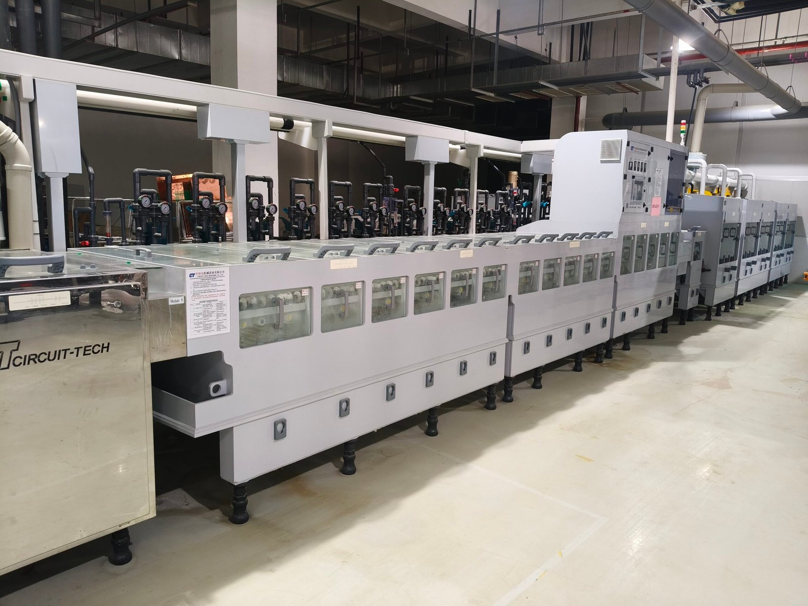
II. Core Structural Composition: Modular Design Ensures Stable Operation
The PCB developing line usually adopts a "horizontal continuous" structure and is divided into five core modules according to functions. Each module collaborates to achieve automated and continuous production:
| Module Name | Core Components | Main Functions |
|---|---|---|
| Infeed | Conveyor rollers, deviation - correcting device, substrate detector | Receives the exposed PCB, and ensures the substrate center is aligned with the conveyor line through the deviation - correcting device to avoid subsequent developing deviation |
| Pre - Wet Tank | Deionized water spray nozzles, temperature controller | Pre - wets the substrate, cleans the surface, and balances the temperature |
| Developing Tank | Developer circulation system, spray nozzles, concentration/temperature sensors, conveyor rollers | Achieves selective dissolution, and monitors and adjusts developer parameters in real - time |
| Rinsing Section | Multi - stage spraying system, ultrasonic generator (optional), water quality monitor | Terminates developing, cleans residues, and ensures the rinsing effect |
| Drying Section | Hot - air generator, infrared heating tubes, wind speed sensor | Quickly dries the substrate to avoid water - mark residues |
| Outfeed | Conveyor rollers, appearance inspection camera (optional) | Outputs the developed PCB. Some lines are equipped with an AOI camera for preliminary detection of developing defects |
| In addition, the developing line is also equipped with a developer replenishment system (monitors the concentration in real - time and automatically replenishes new solution or deionized water), a waste - liquid treatment interface (introduces the developing waste liquid and rinsing wastewater into the environmental protection treatment system), and a PLC control system (integrates parameter setting, real - time monitoring, and fault - alarm functions) to ensure the stable operation of the equipment. |
III. Key Process Control Points and Common Defects
The process stability of the developing line directly determines the PCB pattern accuracy. During production, the following control points need to be closely monitored, and typical defects need to be avoided:
- Key Control Points
- Developer Concentration and Temperature: Detect the concentration once every 15 minutes through an on - line concentration meter (such as a refractometer, conductivity meter), and the temperature sensor monitors the temperature of the developing tank in real - time. An automatic alarm is triggered when the deviation exceeds ±1°C.
- Spray Pressure and Conveyor Speed: Regularly calibrate the spray nozzle pressure (prevent pressure drop due to blockage), and the deviation of the conveyor speed needs to be controlled within ±0.1m/min.
- Rinsing Water Quality and Drying Effect: Monitor the resistivity of fine rinsing water in real - time. After drying, verify the drying effect through a "water - film test" (if a continuous water film is formed after spraying water on the substrate surface, it indicates thorough drying; if water droplets are formed, it indicates the presence of oil stains or incomplete drying).
- Common Defects and Causes
| Defect Type | Performance Characteristics | Main Causes |
| ---- | ---- | ---- |
| Incomplete Developing | Unexposed photoresist remains on the substrate surface (appearing as white fog or dots) | Low developer concentration/temperature, insufficient spray pressure, too fast conveyor speed |
| Over - developing | Fuzzy edges of the circuit pattern, thinner lines (beyond the design tolerance) | High developer concentration/temperature, too long developing time |
| Photoresist Residue | Black/white photoresist debris in circuit gaps and hole walls | Insufficient rinsing pressure, insufficient dissolution of the developer, insufficient exposure of the photoresist |
| Water - mark Residue | White stripes or spots on the substrate surface after drying | Incomplete drying of water after rinsing, insufficient hot - air temperature/wind speed, oil stains on the substrate surface |
IV. Technology Development Trends: Meeting High - Precision and Green Requirements
As PCBs develop towards "high - density (such as HDI, Mini LED PCB) and fine - line (line width/line pitch ≤ 30/30μm)", the technology of the developing line is also continuously evolving. The core trends include:
- Higher - precision Control: Adopting "AI vision + closed - loop control", the AOI camera detects the accuracy of the circuit edges after developing in real - time, and automatically adjusts parameters such as the developer temperature and spray pressure to achieve "adaptive developing".
- Green Upgrade: Developing low - concentration developers (such as 0.8 - 1.2% Na₂CO₃), and recyclable developing systems (by filtering and recovering photoresist residues in the developer to extend its service life), reducing the amount of waste liquid discharged.
- Adaptation to Flexible Substrates: For the bendable characteristics of FPC (flexible PCB), the conveyor rollers of the developing line use "soft silicone rollers", and the spray pressure can be adjusted in sections to avoid substrate wrinkling or damage.
- Intelligent Integration: Accessing the MES system through the industrial Internet, uploading developing parameters and yield data in real - time to achieve full - process traceability. At the same time, a new "fault self - diagnosis" function can automatically identify problems such as spray - nozzle blockage and developer leakage, reducing downtime


