PCB SMT
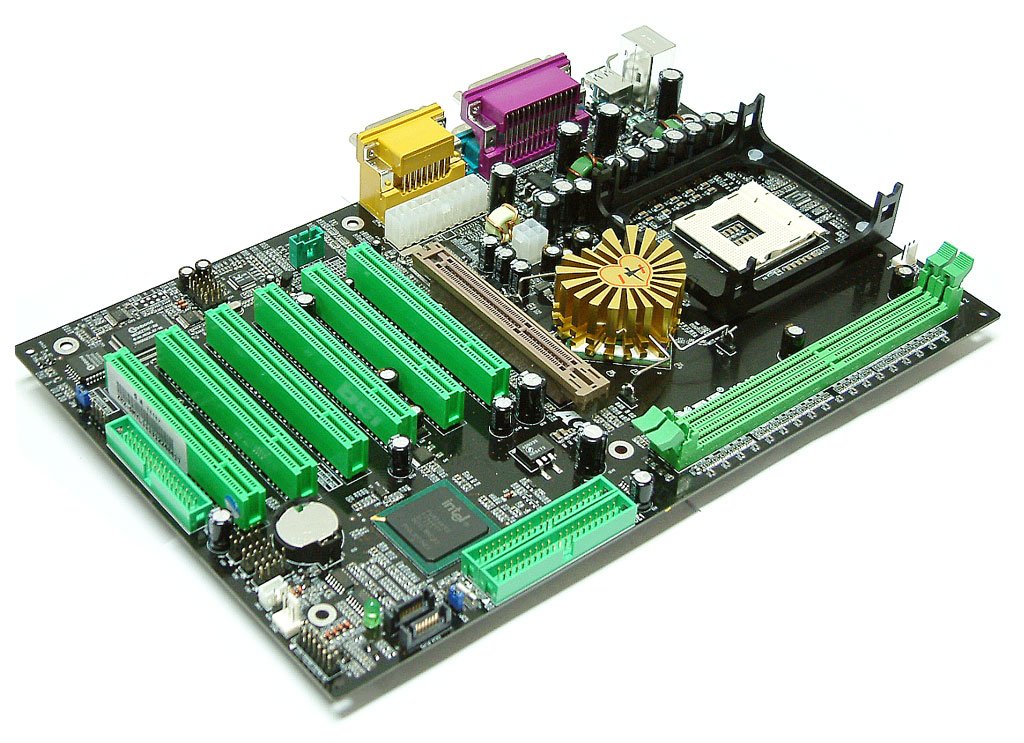
PCB Assembly, abbreviated as PCBA, is a manufacturing process in which a PCB substrate and electronic components like chips, resistors, capacitors, and connectors are soldered and fixed via specific techniques. Eventually, it results in an electronic module with full electrical functionality. It serves as a link between PCB design and mass production of products. It's a crucial step in transforming an electronic device from a "design blueprint" into a "physical product". The quality of its processes directly determines the functional stability, reliability, and service life of the product. PCBA is widely applied in fields such as consumer electronics, industrial control, automotive electronics, and medical equipment.
Get a Quote
PCB Assembly: The Core Manufacturing Link from Substrate to Functional Module
I. The Core Process of PCB Assembly
1. Preparations: Dual Verification of Materials and Processes
- Material Verification: Check the component model (e.g., resistor resistance, capacitor capacitance and voltage rating), package specifications (e.g., 0805 resistor, QFP-64 chip), and pin plating (lead-free/lead-containing) one by one against the BOM (Bill of Materials). At the same time, inspect the PCB substrate for defects such as deformation, scratches, and solder mask peeling to ensure all materials meet design requirements and prevent incorrect or missing use of components.
- Process Parameter Setting: Determine key process parameters based on component characteristics (e.g., maximum temperature resistance of heat-sensitive chips) and PCB specifications (number of layers, copper thickness). For example, the melting point of lead-free solder paste is approximately 217°C, which requires a matching reflow soldering temperature profile; the SMT placement machine’s nozzle must be selected according to the component package (e.g., a 0.3mm diameter nozzle for 0402 resistors) to ensure stable suction.
2. Solder Paste Printing: The "Foundation" for Soldering
Solder paste is a paste-like mixture of solder powder (e.g., Sn96.5Ag3.0Cu0.5) and flux. Its role is to melt at high temperatures to form solder joints, realizing electrical connection between components and PCB pads. The printing process requires precise control of the amount and uniformity of solder paste:
During operation, the PCB is fixed on the printer workbench, and solder paste is screen-printed onto the PCB pads through a stencil (a stainless steel sheet with hollow holes etched according to the pad pattern). The stencil thickness (commonly 0.12-0.15mm) and hole size must match the pads. For example, the stencil hole for an 0805 resistor pad is approximately 0.4mm×0.2mm, ensuring the solder paste amount on each pad is uniform (error ≤10%) without insufficient solder or solder bridging.
After printing, an AOI (Automatic Optical Inspection) device is used to check the position and thickness of the solder paste. If deviations or bridging are found, the paste is cleaned and reprinted promptly to avoid affecting subsequent soldering.
3. Component Mounting: The "Key Step" for Precise Positioning
Component mounting is completed by an SMT placement machine, with the core process of "nozzle suction → visual recognition → precise placement":
The placement machine selects a suitable nozzle based on the component package, captures images of the component and PCB fiducial marks (Mark points) via a CCD camera, compares them with the design coordinates to automatically calibrate the position, and ensures the mounting accuracy (within ±0.02mm, meeting the requirements of QFP chips with 0.5mm pitch).
During placement, the pressure must be controlled (e.g., approximately 0.1N for 0402 resistors and 0.5N for BGA chips). Excessive pressure may damage components or the PCB, while insufficient pressure leads to poor contact between components and solder paste. For oversized connectors and irregular components, manual auxiliary positioning or special jigs are required for fixation.
4. Reflow Soldering: The "Core Process" for Forming Reliable Solder Joints
- Preheating Stage (80-150°C, 60-120s): Heat slowly to remove solvents in the solder paste, preventing bubbles caused by rapid solvent evaporation.
- Soak Stage (150-180°C, 60-90s): Activate the flux to remove oxide layers on the pads and pins, and prevent stress on components due to temperature differences.
- Reflow Stage (Peak temperature 230-250°C, 10-20s): The solder melts and wets the contact surfaces to form alloy solder joints. The peak temperature must be 15-30°C higher than the melting point of the solder paste but not exceed the maximum temperature resistance of components (e.g., most chips can withstand a maximum temperature of 260°C).
- Cooling Stage (Cooling from peak temperature to below 80°C, 60-120s): Cool rapidly to crystallize the solder joints, forming a dense and high-strength soldered structure. Slow cooling is avoided to prevent coarse solder joint grains and reduced reliability.
5. Inspection and Rework: The "Final Line of Defense" for Quality Assurance
- AOI Inspection: Scans the PCBA surface to automatically identify issues such as cold solder joints, missing solder, incorrect/reversed component mounting, and component absence. It is suitable for rapid screening in large-scale mass production.
- X-Ray Inspection: For components with "bottom solder joints" such as BGA and CSP, X-rays penetrate the PCB to check for internal defects in solder joints, such as voids (void rate ≤25%), cold solder joints, and missing solder balls. It is a core method for inspecting invisible solder joints.
- ICT/FCT Testing: ICT (In-Circuit Test) checks circuit continuity and component parameters; FCT (Functional Test) simulates actual operating conditions to test the overall function of the PCBA (e.g., power output voltage, communication signal strength).
- Rework: Use a hot air gun/soldering iron to remove defective components, clean the pads, and re-solder qualified components. The reworked PCBA must be inspected again to confirm quality.
II. Key Requirements and Common Issues in PCB Assembly
1. Core Process Requirements
- Soldering Quality: Solder joints must be full and free of voids, with the wetting area between solder and pads ≥90%. For fine-pitch components (e.g., QFP with 0.4mm pitch), solder bridging between pins must be avoided, and the spacing between adjacent solder joints must comply with design specifications.
- Component Protection: Anti-static measures (wearing anti-static wristbands, using anti-static workbenches) must be implemented throughout the process; mechanical damage (controlling placement pressure, avoiding collisions) and high-temperature damage (not exceeding the maximum temperature resistance of components) must be prevented.
- Cleanliness: Residual flux on the PCBA must be removed after soldering (except for no-clean flux) to avoid PCB corrosion in humid environments or impacts on the insulation of high-voltage circuits.
2. Common Issues and Solutions
- Cold Solder Joints: Caused by insufficient solder paste, oxidized pads, or insufficient reflow soldering temperature. Solutions: Inspect the stencil to ensure sufficient solder paste; clean the oxide layer on pads; adjust the reflow soldering temperature profile.
- Solder Bridging: Caused by excessive solder paste printing or placement machine deviation. Solutions: Reduce the stencil hole size; calibrate the placement accuracy of the placement machine; use solder wick to remove excess solder during rework.
- BGA Solder Joint Voids: Caused by rapid flux evaporation or insufficient preheating. Solutions: Select low-volatility solder paste; extend the preheating time; clean BGA pads and solder balls.
- Reversed Component Mounting: Caused by visual recognition errors or incorrect polarity marking. Solutions: Optimize the recognition parameters of the placement machine; verify the BOM and PCB silkscreen; focus on screening polar components during AOI inspection.
III. Process Selection and Development Trends
1. Basis for Process Selection
- Production Scale: For small-batch prototyping (10-100 units), manual printing + small reflow ovens are used; for large-scale mass production (1,000+ units), high-speed placement machines (60,000 points/hour) + large reflow ovens are adopted to improve efficiency.
- Reliability Requirements: For automotive electronics and medical equipment, lead-free solder paste and high-Tg PCBs (≥150°C) are required, and reliability tests such as temperature cycling and damp heat tests are added.
2. Development Trends
- High-Density Integration: To adapt to miniature components such as 01005 resistors and BGAs with 0.3mm pitch, high-precision placement machines (±0.005mm) and thin stencils (0.08mm) are needed.
- Intelligentization: Introduce AI visual inspection (defect recognition rate 99.9%), automated rework robots, and MES (Manufacturing Execution System) to monitor the production process, reducing manual intervention.
- Green Environmental Protection: Promote lead-free solder, no-clean flux, and recyclable materials to comply with environmental standards such as RoHS and REACH.


