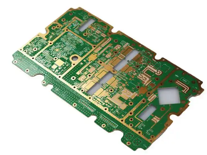
High frequency PCB
High - Frequency PCB is a printed circuit board used in scenarios with high - frequency signals above 300MHz. Its core requirements are low signal loss and high stability. For base materials, PTFE (with a dielectric constant of 2.0 - 2.2 and dielectric loss ≤ 0.001) and BT resin (Dk of 3.0 - 3.5) are often chosen, paired with 1/4 - 1/2OZ ultra - thin copper foil (roughness Ra≤0.5μm). Technologically, it needs to laser - form micro - blind holes (≤0.1mm) and control impedance deviation within ±5%. It is suitable for scenarios like 5G base - stations, radars, and satellite communications, reducing high - frequency signal attenuation and ensuring data - transmission rate and accuracy
Get a Quote
I. Core Judging Criteria of High - Frequency PCBs: What is "True High - Frequency"?
- Frequency Range: In conventional high - frequency scenarios (5G base - stations, WiFi 6), it is mostly 300MHz - 6GHz. In medium - and high - frequency scenarios (millimeter - wave radars, satellite communications), it reaches 24GHz - 110GHz (such as 77GHz automotive radars, 100GHz terahertz communications).
- Signal Loss Requirements: High - frequency signals are prone to attenuation due to dielectric and conductor losses. A qualified high - frequency PCB should meet the requirement that at the target frequency, the Insertion Loss is ≤0.5dB/cm (for example, at 6GHz, the loss of FR - 4 base material is about 0.8dB/cm, while that of PTFE base material is only 0.3dB/cm).
- Impedance Stability: High - frequency signals are extremely sensitive to impedance changes. The characteristic impedance tolerance needs to be controlled within ≤±5% (such as 50Ω single - end impedance, 100Ω differential impedance) to avoid signal reflection caused by impedance mutations.
II. Core Material System of High - Frequency PCBs: The "Cornerstone" of Low Loss
- Base Material (Insulating Core): The Key to Determining High - Frequency LossThe dielectric constant (Dk) and dielectric loss tangent (Df) of the base material are the core indicators. The smaller the Dk, the faster the signal - transmission speed. The smaller the Df, the lower the dielectric loss. There are three main types of base materials:
- PTFE (Polytetrafluoroethylene) Base Material: It represents the pinnacle of high - frequency performance. At 10GHz, Dk = 2.0 - 2.2, and at 25℃, Df ≤ 0.001. It has a high temperature resistance of over 260℃ and extremely strong chemical stability (resistant to acid and alkali corrosion). However, it has a high cost (about 5 - 8 times that of FR - 4) and high processing difficulty (easy to deform, and burrs are likely to occur during drilling). It is suitable for ultra - high - frequency scenarios such as 77GHz millimeter - wave radars and satellite phased - array antennas. Representative models include Rogers RO4835 (Dk = 3.48, Df = 0.0037) and Taconic TLY - 5 (Dk = 2.2, Df = 0.0009).
- BT Resin Base Material: It is a cost - effective choice. At 10GHz, Dk = 3.0 - 3.5, Df = 0.002 - 0.005, with a temperature resistance of 240 - 280℃. Its cost is only 30% - 50% of that of PTFE, and its processing performance is similar to that of conventional FR - 4. It is suitable for medium - and high - frequency scenarios such as 5G base - station RF modules and WiFi 7 routers, and is currently the mainstream choice for high - frequency PCBs in consumer electronics. Representative models include Japan JX's BT - ESL and Nan Ya Plastics' NBT series.
- Modified FR - 4 Base Material: It is an entry - level high - frequency base material. By adding ceramic fillers (such as alumina, boron nitride), the loss is reduced. At 10GHz, Dk = 3.8 - 4.2, Df = 0.008 - 0.012. Its cost is close to that of conventional FR - 4 (only 10% - 20% higher), but its high - frequency performance is limited (the loss increases significantly above 6GHz). It is suitable for medium - and low - frequency scenarios such as 4G base - stations and automotive central - control high - frequency modules, and is an "entry - level alternative solution" for high - frequency PCBs. Representative models include Shengyi Technology's S1130 (Dk = 4.0, Df = 0.008) and Kingboard Group's KB - 6160.
- Copper Foil (Conductive Layer): The Key to Reducing Conductor LossThe "skin effect" of high - frequency signals (current concentrated on the conductor surface) is significant. The roughness (Ra) and thickness of the copper foil directly affect conductor loss:
- Ultra - thin Low - roughness Copper Foil: It is preferred to use 1/4OZ (9μm) or 1/2OZ (17.5μm) electrolytic copper foil with a surface roughness Ra ≤ 0.5μm (Ra of conventional copper foil is approximately 1.2μm), which can reduce the scattering loss of signals on the copper - foil surface. It is suitable for millimeter - wave radars and high - frequency RF circuits. A representative model is JX's HVLP - 1/4OZ (Ra = 0.3μm).
- High - purity Copper Foil: The copper content should be ≥99.98% to avoid signal attenuation caused by impurities (such as iron, zinc). At the same time, the tensile strength of the copper foil should be increased (≥300MPa) to prevent breakage during processing.
- Prepreg (Inter - layer Bonding)It needs to match the resin system of the base material to ensure the consistency of inter - layer dielectric properties:
- PTFE base material is paired with PTFE prepreg (such as Rogers RO4450B), with a Dk difference from the base material ≤0.1.
- BT resin base material is paired with BT prepreg, with the resin content controlled at 55% - 65% to avoid uneven dielectric properties due to excessive resin flow.
- Modified FR - 4 base material is paired with low - loss FR - 4 prepreg, and ceramic fillers are added to reduce inter - layer loss.
III. Core Processes of High - Frequency PCBs: Precise Control to Reduce Signal Interference
- Circuit Manufacturing: High - precision Forming to Reduce Signal Scattering
- LDI Laser - Direct Imaging: It replaces traditional film exposure, with a resolution of 5080dpi (minimum line - width/spacing of 2/2mil, 0.05/0.05mm) and a positioning accuracy of ±1μm, avoiding circuit deviation caused by film deformation.
- Low - temperature Slow Etching: The etchant temperature is reduced to 38±1℃ (conventional 45℃), and the etching rate is controlled at 0.8μm/min (conventional 1.2μm/min). Etching is carried out in three times to compress the under - etching amount from 12μm to less than 5μm, ensuring smooth circuit edges and reducing signal - scattering loss.
- Circuit Edge Treatment: After etching, through the "micro - polishing" process (sandpaper with a mesh number of 1000#), burrs on the circuit edges are removed (≤3μm), further reducing conductor loss.
- Micro - hole Processing: Shortening the Signal Path to Reduce DelayThe longer the high - frequency signal - transmission path, the greater the loss. It is necessary to shorten the inter - layer interconnection distance through "micro - blind holes/buried holes":
- UV Laser Drilling: Micro - blind holes of 0.08 - 0.15mm are processed, with a hole - position deviation of ±0.5μm and a hole - wall roughness Ra ≤ 0.8μm, avoiding the rough hole wall caused by mechanical drilling (Ra of conventional mechanical drilling is approximately 2μm).
- Resin Plugging: For micro - blind holes, the "vacuum filling + hot - air curing" process is used. The plugging resin needs to match the Dk of the base material (with a difference ≤0.2), and the surface flatness is ≤5μm to avoid impedance mutations.
- Back - drilling Process: For high - frequency signal channels (such as 112G SerDes signals), back - drilling is used to remove the redundant copper segments in the holes (residual stub ≤ 0.2mm), eliminating signal - reflection interference and reducing the insertion loss by 15% - 20%.
- Impedance Control: Precise Control throughout the Process
- Design Stage: Through impedance - calculation software (such as Polar SI9000), combined with the Dk of the base material, the thickness of the copper foil, and the thickness of the dielectric layer, the width and spacing of the circuit are designed (for example, for 50Ω single - end impedance, with a PTFE base material (Dk = 2.2), the line - width is 0.2mm, and the dielectric - layer thickness is 0.15mm).
- Manufacturing Stage: The thickness of the dielectric layer (error ±3μm) and the thickness of the copper foil (error ±5%) are monitored in real - time. 20 boards are sampled from each batch, and the impedance is detected with a TDR time - domain reflectometer (tolerance ≤±5%).
- Compensation Measures: For the etched circuit, if the impedance deviation exceeds the tolerance (such as 52Ω), the impedance is adjusted to the qualified range by "locally electro - plating and thickening the copper layer" (increasing the copper thickness by 1 - 2μm).
- Surface Treatment: Balancing Low Loss and Reliability
- Gold - plating Process: The gold - layer thickness is 0.05 - 0.1μm, the nickel - layer thickness is 2 - 3μm, and the gold purity is ≥99.9%. It reduces the contact resistance (≤5mΩ), and the high - frequency loss of gold is low. It is suitable for high - frequency connectors and antenna feed points.
- OSP Process: The thickness of the organic solder - preservative is 0.5 - 1μm. It has a low cost and no high - frequency loss, but its temperature resistance is limited (≤260℃). It is suitable for non - welding areas or low - temperature welding scenarios.
- Selective Surface Treatment: Gold - plating is used for high - frequency signal areas, and OSP is used for non - signal areas, balancing performance and cost. This is common in 5G base - station PCBs.
IV. Typical Application Scenarios of High - Frequency PCBs: From Consumer Electronics to Aerospace
- 5G/6G Communication Field
- 5G Base - stations: The Massive MIMO antenna array uses a BT resin - based PCB, supporting 3.5GHz/26GHz frequency bands, with an insertion loss ≤0.6dB/cm, suitable for large - scale antenna signal transmission.
- 6G Terminals: In the terahertz communication (100GHz) scenario, a PTFE - based PCB is required, with Df ≤ 0.001, supporting 1Tbps ultra - high - speed data transmission. Currently, it is in the research and development stage.
- Automotive Electronics Field
- Millimeter - wave Radars: The 77GHz vehicle - mounted radar uses a PTFE - based PCB, with a line - width/spacing of 3/3mil, a micro - blind - hole aperture of 0.1mm, a detection distance of ≥200m, and an angular accuracy of ≤0.5°.
- In - vehicle Ethernet: The 1000BASE - T1 in - vehicle Ethernet module uses a modified FR - 4 - based PCB, supporting the 1GHz frequency band, with an insertion loss ≤0.8dB/cm, meeting the automotive EMC (electromagnetic compatibility) requirements.
- Aerospace and Defense Field
- Satellite Communications: The phased - array antenna of low - orbit satellites uses a PTFE - based PCB, with a temperature - resistance range of - 55℃~125℃, passing a 2000 - hour salt - spray test, and an insertion loss ≤0.4dB/cm at 20GHz.
- Radar Systems: The air - defense radar uses a Rogers RO4835 - based PCB, supporting the X - band (8 - 12GHz), with an impedance tolerance of ±3%, ensuring the long - distance detection accuracy of radar signals.
- Consumer Electronics Field
- High - end Routers: The WiFi 7 router (6GHz frequency band) uses a BT resin - based PCB, supporting 4096 - QAM modulation, with an insertion loss ≤0.7dB/cm, achieving a 10Gbps wireless rate.
- VR Devices: The millimeter - wave positioning module of VR headsets uses an ultra - thin PTFE - based PCB (thickness of 0.2mm), with a line - width/spacing of 2/2mil, suitable for a narrow installation space.
V. Technical Challenges and Development Trends of High - Frequency PCBs
- Challenge 1: Loss control in ultra - high - frequency scenarios (such as terahertz). In frequency bands above 100GHz, the Df of existing PTFE base materials needs to be further reduced to below 0.0005, and the processing accuracy needs to reach the micron level.
- Challenge 2: High cost. The cost of PTFE - based PCBs is 5 - 8 times that of conventional FR - 4, limiting their large - scale application in consumer electronics.
- Challenge 3: Balancing reliability and performance. In high - temperature and vibration environments (such as the automotive engine compartment), high - frequency PCBs are prone to inter - layer delamination, and the bonding force between the base material and the copper foil needs to be improved.Future development trends focus on three directions:
- Material Innovation: Develop "low - Dk + low - cost" base materials (such as modified PTFE and glass - fiber composite base materials), reducing the cost by more than 30%.
- Process Upgrade: Introduce technologies such as "laser - direct structuring (LDS)" and "3D printing" to achieve the integrated forming of complex high - frequency structures, reducing signal loss.
- Integration: Integrate high - frequency PCBs with antennas and filters (such as AIP antenna packaging), shortening the signal path and improving the device integration.
Lorem ipsum dolor sit amet, consectetur adipiscing elit. Ut elit tellus, luctus nec ullamcorper mattis, pulvinar dapibus leo.Lorem ipsum dolor sit amet, consectetur adipiscing elit. Ut elit tellus, luctus nec ullamcorper mattis, pulvinar dapibus leo.Lorem ipsum dolor sit amet, consectetur adipiscing elit. Ut elit tellus, luctus nec ullamcorper mattis, pulvinar dapibus leo.Lorem ipsum dolor sit amet, consectetur adipiscing elit. Ut elit tellus, luctus nec ullamcorper mattis, pulvinar dapibus leo.
Lorem ipsum dolor sit amet, consectetur adipiscing elit. Ut elit tellus, luctus nec ullamcorper mattis, pulvinar dapibus leo.Lorem ipsum dolor sit amet, consectetur adipiscing elit. Ut elit tellus, luctus nec ullamcorper mattis, pulvinar dapibus leo.Lorem ipsum dolor sit amet, consectetur adipiscing elit. Ut elit tellus, luctus nec ullamcorper mattis, pulvinar dapibus leo.Lorem ipsum dolor sit amet, consectetur adipiscing elit. Ut elit tellus, luctus nec ullamcorper mattis, pulvinar dapibus leo.

Lorem ipsum dolor sit amet, consectetur adipiscing elit. Ut elit tellus, luctus nec ullamcorper mattis, pulvinar dapibus leo.Lorem ipsum dolor sit amet, consectetur adipiscing elit. Ut elit tellus, luctus nec ullamcorper mattis, pulvinar dapibus leo.Lorem ipsum dolor sit amet, consectetur adipiscing elit. Ut elit tellus, luctus nec ullamcorper mattis, pulvinar dapibus leo.Lorem ipsum dolor sit amet, consectetur adipiscing elit. Ut elit tellus, luctus nec ullamcorper mattis, pulvinar dapibus leo.
Lorem ipsum dolor sit amet, consectetur adipiscing elit. Ut elit tellus, luctus nec ullamcorper mattis, pulvinar dapibus leo.
Lorem ipsum dolor sit amet, consectetur adipiscing elit. Ut elit tellus, luctus nec ullamcorper mattis, pulvinar dapibus leo.


