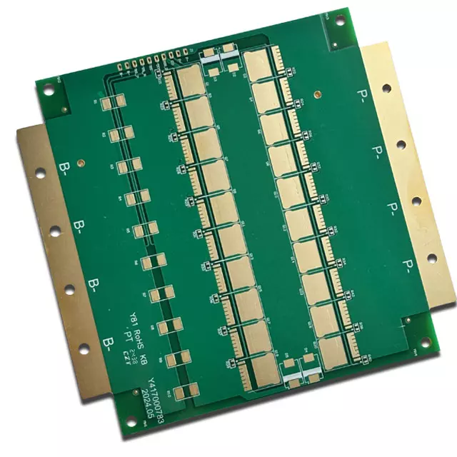
HDI PCB
四层铜基电路板是一种具有高效散热和复杂布线能力的印刷电路板。其核心结构是“铜导电层+绝缘导热层”的交替堆叠(总共四层功能层)。顶层和底层的铜箔(18-70μm)用于焊接功率器件和传输信号。中间的铜层可以实现电路互连或屏蔽。绝缘层主要使用陶瓷填充树脂(导热系数为1-5W/m·K),以确保快速散热。
它结合了高密度布线(支持多环路电路设计)和强大的散热能力(散热效率比双层铜基电路板提高30%以上)。它广泛应用于LED照明、汽车电源模块和工业电源等场景。它能有效解决高功率器件的散热积聚问题,提高设备的稳定性和使用寿命。
Get a Quote
I. Core Process Flow: Step - by - step Realization from Base Material to Finished Product
The production of four - layer copper - based circuit boards needs to focus on two goals: "copper - layer conduction" and "stability of the insulating and heat - conducting layer". The process proceeds in the order of "base - material preparation → lamination → drilling and via metallization → circuit formation → surface treatment → shape processing". Each step requires strict matching of material properties and process parameters.
(1) Base - material Preparation: Laying the Foundation for Heat - dissipation and Conductivity
The choice of base materials directly determines the core performance of four - layer copper - based circuit boards. Copper foils and insulating and heat - conducting base materials need to be prepared separately and pre - treated.
- Copper Foil Selection and Treatment: Select electrolytic copper foils with a purity of ≥99.9% (common thicknesses are 18μm, 35μm, 70μm). The top - layer and bottom - layer copper foils should meet the soldering requirements of power devices (preferably with a thickness of 35μm or more), and the two middle - layer copper foils focus on circuit interconnection (18μm thin copper foils can be selected). In the pre - treatment stage, through "degreasing cleaning (removing surface oil stains) → pickling (5% sulfuric acid solution to remove the oxide layer) → passivation treatment (forming a nano - level protective film)", ensure that the surface roughness of the copper foil Ra ≤ 1.5μm to improve the bonding force with the insulating layer.
- Insulating and Heat - conducting Base - material Preparation: Corely use ceramic - filled epoxy resin base materials (thermal conductivity of 1 - 5W/m·K, suitable for medium - to - high - power scenarios) or aluminum nitride ceramic base materials (thermal conductivity of 150 - 200W/m·K for high - end heat - dissipation requirements). Cut the base material to the designed size (with an error of ±0.1mm), and through "plasma cleaning (removing surface impurities) → pre - heating (80℃ for 30min to remove internal moisture)", avoid bubbles in subsequent lamination.
(2) Lamination: Integrating the Four - layer Structure
Lamination is a key process to form the alternating structure of "copper layer - insulating layer - copper layer", and the problem of "mismatch of thermal expansion coefficients of different materials" needs to be solved. First, stack in a clean room (Class 1000) in the order of "bottom - layer copper foil → insulating and heat - conducting base material → middle copper foil → insulating and heat - conducting base material → top - layer copper foil", and lay a "bonding film" (modified epoxy resin, thickness of 0.05 - 0.1mm) between each layer. Then, send it to a vacuum laminator and adopt a "step - by - step temperature - increasing and pressure - increasing" process:
- Pre - heating Stage: From 60℃ to 100℃, with a heating rate of 5℃/min, a pressure of 5kg/cm², and keep warm for 20min to remove the air between layers.
- Curing Stage: From 100℃ to 160℃, with a heating rate of 3℃/min, a pressure of 20 - 25kg/cm², and keep warm for 60min to ensure that the bonding film is completely cured.
- Cooling Stage: Naturally cool to room temperature (with a cooling rate of ≤4℃/min) to prevent internal stress in the base material due to temperature differences. After lamination, test the inter - layer bonding force (peel strength ≥ 1.2N/mm) to ensure there are no delamination or bubble defects.
(3) Drilling and Via Metallization: Establishing Inter - layer Electrical Interconnection
Four - layer copper - based circuit boards need to achieve the conduction of each copper layer through drilling and via metallization. The process is divided into four steps: "drilling → hole - wall treatment → electroless copper plating → electro - plating copper".
- Drilling: According to design requirements, use a CNC drilling machine to drill "through - holes" (hole diameter 0.3 - 0.8mm, suitable for through - hole components) and "blind holes" (hole diameter 0.1 - 0.3mm for local layer interconnection). The drilling accuracy needs to be controlled within ±0.02mm, and the hole - wall roughness Ra ≤ 2.5μm to avoid burrs affecting subsequent metallization.
- Hole - wall Treatment: Through "alkaline degreasing (removing drilling oil stains) → acidic etching (removing resin burrs on the hole wall) → plasma cleaning (activating the hole - wall surface to improve the adhesion of electroless copper plating)", ensure that the hole wall is clean and free of impurities.
- Electroless Copper Plating and Electro - plating Copper: First, use the electroless copper - plating process (copper sulfate solution, at 45℃ for 20min) to form a 0.5 - 1μm thick conductive layer on the hole wall. Then, through electro - plating copper (nickel sulfate plating solution, with a current density of 2A/dm² for 60min), increase the copper thickness on the hole wall to 20 - 30μm, ensuring that the hole resistance ≤ 5mΩ to meet the current - transmission requirements.
(4) Circuit Formation: Precision Fabrication of Conductive Circuits
Circuit formation needs to pattern the copper layer through "dry - film exposure → development → etching", with the core being to ensure circuit accuracy and edge smoothness.
- Dry - film Lamination: Laminate the photosensitive dry - film (thickness of 25 - 35μm) onto the substrate surface through hot - pressing (at 80℃ with a pressure of 0.5kg/cm²) to ensure there are no bubbles or wrinkles.
- Exposure and Development: Use an ultraviolet exposure machine (exposure energy of 80 - 120mJ/cm²) to expose according to the circuit film pattern, and then develop with a sodium carbonate solution (1% concentration, at 30℃) to remove the unexposed dry - film, exposing the copper layer to be etched.
- Etching: Use a ferric chloride solution (concentration of 400g/L, at 50℃) to etch the exposed copper layer. Control the etching rate at 2μm/min to ensure there is no under - etching at the circuit edges (under - etching amount ≤ 5μm), and control the line - width error within ±10% (for example, if the designed line - width is 0.2mm, the actual error should be ≤ ±0.02mm). After etching, peel off the remaining dry - film and use AOI (Automated Optical Inspection) to check for open - circuits, short - circuits, line - width deviations, etc.
(5) Surface Treatment and Shape Processing: Improving Practicality and Adaptability
- Surface Treatment: Select different processes according to application scenarios. Use "gold - plating" (gold thickness of 1 - 3μm, nickel thickness of 5 - 8μm to improve soldering reliability) for the soldering area, and use "solder - mask ink printing" (epoxy resin solder - mask, thickness of 20 - 30μm for insulation and anti - oxidation) for non - soldering areas. After printing, cure at 150℃ for 60min to ensure adhesion (cross - cut test ≥ 4B level).
- Shape Processing: Use a CNC punching machine (for simple shapes) or laser cutting (for complex shapes) to process according to the designed size. Control the cutting accuracy within ±0.05mm, and ensure there are no burrs at the edges (burr height ≤ 0.02mm). If mounting holes are required, drill again and perform "hole - mouth chamfering" (45° angle, 0.1mm depth) to avoid sharp corners scratching components.
II. Key Technical Difficulties: Breaking through the Synergy Bottleneck of Performance and Process
There are three core technical difficulties in the production of four - layer copper - based circuit boards, which need to be solved one by one through process optimization:
- Bonding Stability between the Insulating and Heat - conducting Layer and the Copper Foil: The thermal expansion coefficients of the insulating layer (such as ceramic - filled resin) and the copper foil are quite different (the thermal expansion coefficient of resin is about 30ppm/℃, and that of copper is about 17ppm/℃), and delamination is likely to occur during lamination. It is necessary to "pre - treat the copper - foil surface (increase roughness) + optimize the bonding - film formula (introduce flexible modifiers) + control the laminating cooling rate" to improve the inter - layer bonding force. Also, there should be no delamination after the high - and low - temperature cycling test (-40℃ to 125℃, 100 cycles).
- Reliability of Via Metallization: The drilling depth of the four - layer structure is large (50% more than that of double - layer boards), and resin burrs or impurities are likely to appear on the hole wall, resulting in the breakage of the electroless copper - plating layer. It is necessary to introduce "plasma cleaning + acidic etching" double hole - wall treatment, and optimize the electroless copper - plating process parameters (such as extending the electroless copper - plating time to 25min) to ensure that the copper layer on the hole wall is continuous without breakpoints. After the "thermal shock test" (260℃ for 10s, 3 times), there should be no significant change in the hole resistance.
- Precision Control of Circuit Etching: The middle copper foil is thin (such as 18μm), and over - etching is likely to occur during etching, making the circuit thin and weak. It is necessary to adopt "low - concentration etchant (ferric chloride concentration of 350g/L) + slow etching rate (1.5μm/min) + real - time monitoring of etching time", combined with LDI (Laser - direct Imaging) technology (exposure accuracy of ±5μm) to ensure the integrity of fine - line - width (such as 0.1mm) circuits.
III. Quality - control System: Ensuring Product Performance throughout the Process
Four - layer copper - based circuit boards need to establish a quality - control system covering "raw materials - processes - finished products":
- Raw - material Inspection: Test the purity, tensile strength (≥250MPa), and elongation (≥10%) of copper foils; test the thermal conductivity (error ≤ 10%) and temperature resistance (no deformation at 260℃) of insulating base materials.
- Process Inspection: After lamination, test the inter - layer bonding force and bubbles; after via metallization, use X - Ray to test the copper - layer thickness on the hole wall; after circuit formation, the AOI inspection qualification rate should be ≥99.5%.
- Finished - product Inspection: Include electrical - performance testing (insulation resistance ≥ 10¹⁰Ω, withstand voltage ≥ 500V AC), heat - dissipation performance testing (thermal resistance ≤ 0.5℃/W), and mechanical - performance testing (flexural strength ≥ 150MPa) to ensure that the finished products meet IPC - 4101 (base - material standard) and IPC - 6012 (circuit - board standard).


