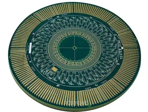
32 layer IC test pcb
The 32 - layer IC test PCB board serves as the core for high - end integrated circuit testing, emphasizing high - density interconnection and high - precision signal transmission. With an alternating lamination of "signal layer - ground layer - power layer", it has multiple independent test loops, enabling synchronous testing of 32 or more ICs. The board integrates micro - probe interfaces and impedance - matching networks (50Ω/75Ω), suitable for the function, timing, and performance tests of complex ICs like CPUs and FPGAs. High - Tg FR - 4 base materials (Tg≥180℃) are selected. By passing strict signal integrity tests, it ensures accurate test data, catering to semiconductor R & D and mass - production quality inspection processes.
Get a Quote
I. Base - material Pretreatment: Guarantee for High - frequency and Low - loss
Modified FR - 4 base materials with a high Tg (≥180℃) and low loss (Df≤0.002@10GHz) are selected. The dielectric constant is controlled at 3.8±0.2 to ensure stable high - frequency signal transmission. In the pretreatment stage:
- After CNC cutting (with an accuracy of ±0.05mm), perform plasma cleaning (in an oxygen atmosphere, with a power of 800W for 3min) to remove surface organic impurities.
- Bake in a vacuum at 120℃ for 4h to control the water content of the base material below 0.02%, avoiding bubbles in subsequent lamination.
- Select electrolytic copper for the copper foil (with a thickness of 12μm) with a surface roughness Ra≤0.3μm to reduce high - frequency signal transmission losses.
II. Inner - layer Fabrication: Ultra - fine Circuit Formation Technology
For the 32 - layer board, 16 groups of inner - layer core boards need to be fabricated first. The core process focuses on the precision control of ultra - fine circuits:
- Choose a 5μm ultra - thin photosensitive film for the dry - film. Use electrostatic adsorption + hot - pressing (60℃, 0.3kg/cm²) for lamination to ensure no bubbles.
- Use LDI laser exposure (with a wavelength of 355nm and a positioning accuracy of ±2μm). The edge roughness of the 30μm line - width / 30μm line - spacing pattern should be ≤3μm.
- After alkaline development (1.0% sodium carbonate, 28℃), adopt a micro - etching process (ammonium persulfate solution, with an etching amount of 0.5μm) to avoid under - etching.
- The AOI inspection is equipped with a 5μm resolution camera to identify open - circuits, short - circuits, and line - width deviations (a deviation exceeding ±3μm is judged as a defect).
- The blackening treatment uses a nano - level oxidation process to form a 0.1μm thick oxide layer, with an inter - layer peel strength of ≥1.8N/mm.
III. Lamination Integration: Precise Interconnection of 32 Layers
Lamination is the core link determining the performance of the 32 - layer board. It needs to solve the problems of multi - layer alignment and resin filling:
- The lamination adopts a "signal - ground - power" symmetrical structure. Three groups of optical positioning targets with a diameter of 0.1mm are set on each layer.
- In a vacuum laminator, the CCD vision system is used to achieve precise alignment of 16 groups of core boards, with a cumulative error of ≤15μm.
- Select a low - flow prepreg (PP) (with a fluidity of 10 - 15%), a dielectric constant of 4.0±0.1, and a thickness deviation of ≤5μm.
- The stepped lamination curve: 60℃/10min (pre - heating) → 120℃/30min (10kg/cm², resin flowing) → 180℃/90min (30kg/cm², curing), with a cooling rate of ≤2℃/min.
- After lamination, use X - Ray to detect inter - layer misalignment. The deviation of each layer should be ≤5μm; otherwise, it will be scrapped.
IV. Drilling and Via Metallization: Guarantee for Micro - interconnection Reliability
The 32 - layer board contains a large number of blind and buried holes (with a diameter of 50 - 100μm). Via metallization needs to break through the problem of the depth - diameter ratio:
- Use laser drilling (a UV laser with a wavelength of 355nm) to process blind holes. The hole - wall roughness Ra≤1μm, and the hole - diameter deviation is ±5μm.
- Use mechanical drilling (a tungsten - steel drill bit with a diameter of 0.15 - 0.3mm) to process through - holes, with a rotation speed of 120000rpm and a feed of 0.5m/min.
- Hole - wall treatment: Plasma desmear (a CF4/O2 mixed gas for 5min) → micro - etching (a sulfuric acid / hydrogen peroxide system, with an etching amount of 1μm).
- Electroless copper plating (with a palladium catalyst, a copper - plating thickness of 0.5μm) → electro - plating copper (with a current density of 1A/dm², a hole - copper thickness of ≥20μm), ensuring a hole resistance of ≤2mΩ.
- Use hole - wall integrity inspection (metallographic sectioning + SEM scanning) to ensure no voids, pinholes, etc.
V. Outer - layer Processing: Optimization of High - frequency Signal Performance
The outer - layer needs to achieve precise impedance control of 50Ω/75Ω. The key process points are:
- The outer - layer circuit adopts the semi - additive process (SAP): Thin the copper foil (etch to 5μm) → tin - plating pattern → copper - plating (30μm line - width) → remove tin, with a line - width accuracy of ±2μm.
- Impedance adjustment: By controlling the thickness of the dielectric layer (with an error of ±3μm) and the copper thickness (with an error of ±1μm), control the impedance error within ±5%.
- Use photosensitive low - loss solder - mask ink (Df≤0.003) with a thickness of 10 - 15μm, and use laser to open windows (with an accuracy of ±5μm).
- Surface treatment: Use electroless gold - plating for the test pads (with a gold thickness of 0.8 - 1.2μm and a nickel thickness of 5 - 8μm), with a contact resistance of ≤10mΩ.
- Cut the shape with a laser (with an accuracy of ±10μm), and the edge burrs should be ≤2μm to avoid signal - transmission interference.
VI. Finished - product Inspection: Comprehensive Performance Verification
The 32 - layer IC test board needs to pass strict inspections to ensure test accuracy:
- Electrical Performance: Use a flying - probe test (with an accuracy of ±1μm) to detect open - circuits and short - circuits. Use a TDR time - domain reflectometer to measure impedance (50Ω/75Ω).
- Signal Integrity: Use a vector network analyzer to test the insertion loss (≤1dB@20GHz) and return loss (≥15dB@20GHz).
- Environmental Reliability: After 1000 thermal shock cycles from - 55℃ to 125℃, the impedance change rate should be ≤5%.
- Microscopic Inspection: Randomly select 5% of the products for metallographic sectioning to observe the inter - layer bonding and hole - wall conditions.
- Function Testing: Mount a standard IC for 32 - channel synchronous testing, with a data consistency error of ≤0.1%.
The process flow of the 32 - layer IC test PCB board achieves the core characteristics of "high - density, high - precision, and high - stability" through the fine - tuned control of 128 processes. It provides a reliable carrier for the R & D testing and mass - production quality inspection of 7nm and below advanced - process ICs, promoting the continuous upgrade of semiconductor industry testing technology


