PCB Design
PCB Schematic Diagrams and Design: A Full - process Analysis from Circuit Logic to Practical Implementation
PCB schematic diagrams and design are the core aspects of electronic device R & D. The former is "a blueprint defining circuit logic", while the latter is "an engineering practice of transforming the blueprint into a physical PCB". These two are closely connected and jointly determine the functional realization, performance stability, and production feasibility of the circuit. They run through the entire life - cycle from conceptual design to product debugging and are the core skill set of hardware engineers.
Get a Quote
PCB Schematic and Design: A Comprehensive Analysis from Circuit Logic to Physical Implementation
PCB schematic and design are core links in the R&D of electronic devices. The former serves as the "blueprint defining circuit logic," while the latter is the "engineering practice that transforms the blueprint into a physical PCB." Closely connected, they jointly determine the functional realization, performance stability, and production feasibility of circuits, spanning the entire lifecycle from conceptual design to final product debugging—and form the core skill set for hardware engineers.
I. PCB Schematic: The "Top-Level Design" Defining Circuit Logic
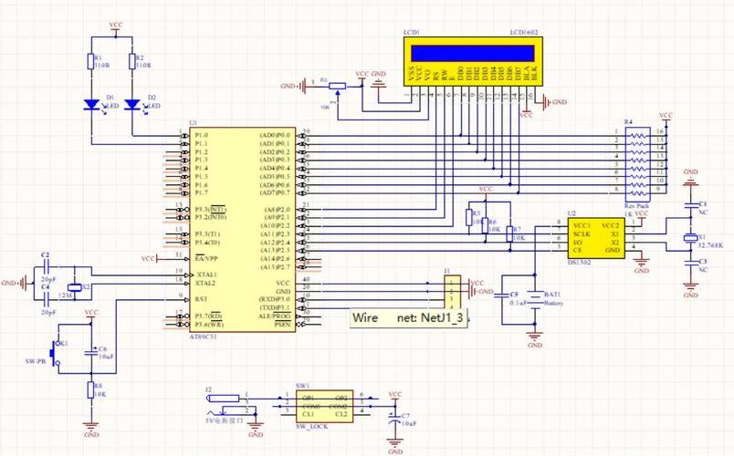
A PCB schematic (Schematic Diagram) is a technical document that uses standardized graphical symbols to intuitively present the electrical connection relationships, signal flow, and functional modules of electronic components. It does not focus on the physical size or layout position of components, but solely on "how to achieve the target function through electrical connections." As the "first step" in the design process, it is the foundation for all subsequent work.
1. Core Components of a Schematic
A standardized schematic must include three core modules—"graphical symbols, connection relationships, and auxiliary information"—to ensure clear logic and complete information:
- Electronic Component Symbols: Compliant with international standards (e.g., IEC 60617, ANSI Y32.2), each component has a dedicated symbol: resistors are represented by "□" (surface-mount) or "—┬—" (through-hole); capacitors by "—||—" (non-polarized) or "—┳—" (polarized); and chips by "rectangle + pins" (e.g., the DIP-20 package symbol for MCUs). Next to each symbol, a reference designator (e.g., R1, C2, U1, uniquely identifying a single component), parameter specifications (e.g., R1 labeled "1kΩ 0805," U1 labeled "STM32F103C8T6"), and package model (e.g., 0805, SOIC-8) must be marked.
- Electrical Wires and Net Labels: Solid lines connect component pins, representing the transmission path of current/signals. For complex circuits (e.g., cross-page or long-distance connections), "net labels" (e.g., "VCC_5V," "SDA_I2C") are used for simplification—nodes with the same label are considered "electrically connected," avoiding clutter from crossed wires.
- Auxiliary Information: Includes a title block (project name, version number, design date, designer information), a bill of materials (BOM) draft (listing reference designators, models, parameters, and packages), annotation text (e.g., "This resistor must withstand 125°C," "Measure voltage at TP1 during debugging"), and functional module zoning (e.g., dashed boxes dividing "power module," "RF module," and "control module").
2. Core Principles of Schematic Design
- Logic Priority, Clear Zoning: Split the circuit into modules by function (e.g., power supply, MCU, sensor, interface) and arrange similar modules centrally (e.g., power module on the left, signal module on the right) to avoid crossed wires between different functions. For example, in a 5V voltage regulation circuit, the input filter capacitor, voltage regulator chip (e.g., 7805), and output filter capacitor should be placed adjacent to each other to intuitively reflect the "input → regulation → output" logic.
- Accurate Parameters, Compliance with Standards: Component parameters must meet circuit requirements with safety margins—for instance, wires in a 1A current loop should have a cross-sectional area of ≥1mm² (labeled "wire diameter ≥1mm²" in the schematic), and capacitors in a 220V AC circuit should have a voltage rating of ≥400V. Additionally, mark characteristics of key signals (e.g., "UART_TX baud rate 9600bps," "ADC input range 0-3.3V").
- Testability and Maintainability: Add test points (TP, labeled "TP1 VCC_3.3V") at key nodes (e.g., power output, signal input) for easy debugging and measurement. Design easily damaged components (e.g., fuses, ESD protection diodes for interfaces) with replaceable through-hole packages to avoid soldering during maintenance.
3. Common Schematic Design Tools
Mainstream tools support core functions such as "symbol library access, ERC checking, and netlist generation"; the choice depends on project scale and team habits:
- Altium Designer: Full-featured, supporting seamless integration from schematic to PCB Layout, with a built-in massive component library (e.g., symbols for TI, ADI chips). Suitable for medium-to-large projects (e.g., industrial control, automotive electronics) but requires payment.
- KiCad: Open-source and free, with customizable symbol and package libraries and rich community resources (e.g., open-source libraries on GitHub). Suitable for small-to-medium projects, students, or startups, with strong compatibility (supports exporting Gerber, BOM, etc.).
- Eagle: A lightweight tool with simple operation, suitable for simple circuits (e.g., Arduino expansion boards). However, it lacks advanced functions (e.g., high-speed signal simulation) and is now owned by Autodesk, requiring a subscription.
II. PCB Design: The "Engineering Practice" Transforming Schematic to Physical Form
PCB design (PCB Layout) is the process of completing "component placement, routing, rule setting, and file output" in PCB design software based on a netlist (containing component packages and connection relationships) generated from the schematic. Its core goal is to "realize the function defined by the schematic while meeting electrical performance, mechanical dimensions, and production process requirements"—and it is the key link determining the final performance and reliability of the PCB.
1. Core Process of PCB Design
(1) Preparations: Clarify Design Constraints
Before formal Layout, define "hard constraints" to avoid repeated modifications later:
- Mechanical Dimensions: Determine the PCB’s length, width, shape (e.g., circular, irregular), and the position/size of mounting holes (e.g., φ3mm mounting holes with a center distance of 50mm) based on product casing or installation requirements.
- Electrical Constraints: Specify power voltages (e.g., 3.3V, 5V, 12V), maximum current (e.g., USB ports must carry 2A), high-speed signal requirements (e.g., DDR3 memory requires impedance control of 50Ω±10%), and EMC (Electromagnetic Compatibility) requirements (e.g., medical devices must meet EN 60601-1).
- Process Constraints: Confirm the number of PCB layers (e.g., single/double-layer, 4-layer), substrate material (e.g., FR-4 epoxy glass cloth substrate; Rogers material for high-frequency circuits), copper thickness (e.g., 1oz copper; 2oz copper for high-current loops), solder mask color (e.g., green, black), and silkscreen color (e.g., white).
(2) Component Placement: "Whole Before Part, Core Before Periphery"
Placement is the first step in PCB design, directly affecting routing difficulty and electrical performance. It must follow the principles of "function priority, shortest signal path, and reasonable heat dissipation":
- Zoned Placement: Divide the PCB into regions by schematic function modules—for example, in a 4-layer board, place signal components (e.g., MCU, sensors) on the Top Layer, interfaces/connectors on the Bottom Layer, use Inner Layer 1 as the GND (ground) plane, and Inner Layer 2 as the VCC (power) plane. Avoid placing power modules adjacent to sensitive signal modules (e.g., RF, ADC) to reduce interference.
- Prioritize Core Components: First place "non-movable" or "core" components—e.g., main chips (CPU, FPGA, which should be close to heat sinks/fans for heat dissipation) and connectors (e.g., USB, HDMI, which must align with casing openings)—then place peripheral components (e.g., resistors, capacitors, inductors). For example, an MCU’s crystal oscillator should be within 5mm of its XTAL pins to reduce clock signal interference.
- Heat Dissipation and Mechanical Compatibility: Place high-power components (e.g., DC-DC converters, power resistors) away from heat-sensitive components (e.g., temperature sensors, MCU) and reserve sufficient heat dissipation space (e.g., no components around power resistors, or design heat-dissipating copper pads). Ensure component placement avoids conflicts with mounting holes/screws, and that the pin spacing of through-hole components meets soldering process requirements (e.g., spacing ≥2.54mm).
(3) Routing: "Meet Rules, Optimize Performance"
Routing connects component pins according to the netlist and must strictly comply with "electrical rules" and "signal integrity" requirements. Key points include:
- Rule Setting: Preset routing rules in the software—trace width (e.g., 0.5mm for 3.3V/1A loops, 1mm for 220V AC), impedance (e.g., 50Ω for high-speed signals, 90Ω for differential signals), spacing (e.g., ≥0.2mm between power and GND, ≥1mm between high and low voltage), and vias (e.g., φ0.3mm vias matching trace width).
- Classified Signal Handling:
- Power Signals: Use "thick traces + copper pouring" (e.g., 1mm traces for 5V/2A power, or direct copper pouring) to avoid excessive voltage drop from high trace resistance. Route multiple power loops separately (e.g., no crossing between 3.3V and 12V traces) and add filter capacitors (e.g., 100nF ceramic capacitors) near component power pins.
- High-Speed Signals (e.g., USB3.0, Ethernet): Use differential routing (two signal traces with equal length, equal spacing, and fixed pitch), avoid vias (to reduce signal reflection), control length difference within 5mil (1mil=0.0254mm), and keep away from power noise sources (e.g., DC-DC converters).
- Sensitive Signals (e.g., ADC input, analog audio): Adopt "single-point grounding" (connecting to the GND plane at only one end to avoid ground loops), route away from digital signal traces (e.g., MCU I/O ports), and add GND copper pour around signal traces for "shielding."
- Routing Optimization: Avoid "acute-angle routing" (use ≥45° angles to reduce signal reflection), avoid "cross-partitioning" (e.g., signal traces should not cross GND plane splits to prevent increased ground impedance), and minimize vias (each via increases signal loss by approximately 0.1dB).
(4) Post-Routing Inspection and File Output
After routing, conduct multiple rounds of inspection to ensure design accuracy:
- Design Rule Check (DRC): The software automatically detects violations of preset rules (e.g., insufficient trace width, excessive spacing, unconnected nets).
- Signal Integrity Simulation: Simulate high-speed signals (e.g., DDR, PCIe) to verify impedance matching and timing compliance, avoiding signal overshoot and ringing.
- 3D Preview: Use the software’s 3D function to check for assembly conflicts between the PCB, casing, and components (e.g., component height exceeding casing limits).
- File Output: Generate production-ready files—Gerber files (core files for PCB manufacturing, containing trace, solder mask, and silkscreen data), BOM (component procurement list with models, quantities, and suppliers), Pick and Place Files (for SMT machine component positioning), and Drill Files (marking via and mounting hole sizes).
2. Key Considerations for PCB Design
- Grounding Design: Proper grounding is critical for interference suppression and circuit stability—separate analog ground (AGND) and digital ground (DGND) and connect them at a single point (e.g., via 0Ω resistors or ferrite beads). Use thick traces or copper pour for high-current ground (e.g., power ground PGND) and avoid sharing it with signal ground to prevent signal interference from voltage drops caused by large currents.
- EMC Optimization: Reduce electromagnetic radiation and susceptibility—add common-mode inductors, X-capacitors, and Y-capacitors to power loops (e.g., at AC-DC power inlets); add GND copper pour around sensitive signals with multi-point grounding; route clock signals on inner layers or use shielded wires to avoid exposure on the Top/Bottom Layers.
- Production Feasibility: Design in line with PCB manufacturing processes—trace width ≥0.2mm (standard process), via diameter ≥0.3mm, silkscreen characters ≥0.8mm×0.8mm (for readability). Avoid "island copper" (unconnected copper that may peel off during soldering) and add thermal vias to large copper areas to prevent warping during soldering.
III. Collaboration Between Schematic and PCB Design: Ensuring "Logic-Physical Consistency"
Schematic and PCB design are not independent; their close collaboration prevents "design disconnect":
- Netlist Synchronization: After modifying the schematic, regenerate the netlist and import it into the PCB design software to update component connections. Failure to synchronize may cause mismatches (e.g., a deleted resistor still remains in the PCB layout).
- Cross-Probing: Use the software’s "Cross Probe" function—clicking a component or net in the schematic highlights the corresponding element in the PCB, enabling quick error localization (e.g., matching "U1 Pin PA0" in the schematic to "U1 Pin 10" in the PCB).
- BOM Synchronization: After PCB design, compare the schematic BOM and PCB BOM to ensure consistency in component models, packages, and quantities (e.g., R1 labeled "0805 1kΩ" in the schematic must not be mistakenly set to "0603 1kΩ" in the PCB).
- Debugging Feedback: If issues (e.g., signal interference, unstable power) are found during PCB prototyping, modify both the schematic and PCB simultaneously—for example, if ADC signal interference is excessive, add an RC filter circuit to the schematic and adjust component placement/routing in the PCB.
IV. Common Issues and Solutions
| Issue Type | Cause | Solution |
|---|---|---|
| ERC error: "Unconnected Net" | Component pins not wired; net label typos (e.g., "VCC_5v" vs. "VCC_5V") | Check unconnected pins; standardize net label case/format; mark unused pins (e.g., chip NC pins) as "floating" with "NC" labels. |
| "Unroutable" PCB Traces | Overcrowded placement; overly strict rules (e.g., excessive trace width/spacing) | Optimize placement (e.g., increase component spacing); adjust rules (e.g., reduce non-critical trace width from 0.3mm to 0.2mm); use vias for layer changes. |
| Power Short Circuit During Debugging | Accidental power-GND connection in the schematic; insufficient power-GND trace spacing in PCB | Re-run schematic ERC; set power-GND spacing to ≥0.5mm in PCB; verify Gerber files before prototyping. |
| High-Speed Signal Transmission Errors | Unequal differential trace lengths; impedance mismatch; proximity to interference sources | Adjust differential trace lengths (use software "length matching" function); control impedance (calculate via trace width/dielectric thickness); keep away from power modules/clock signals. |
Conclusion
The PCB schematic is the "top-level design defining circuit logic," determining "what to do"; PCB design is the "engineering practice realizing logic," determining "how to do it." Complementary and indispensable, a high-quality schematic provides clear direction for PCB design, while standardized PCB design transforms schematic logic into a reliable physical product. For hardware engineers, mastering the core methods of schematic and PCB design—combined with flexible tool application—is key to ensuring electronic devices meet functional, performance, and production requirements, and the only path from "circuit concept" to "physical product."
PCB Schematic and Design: A 1500-Word Overview
From Logical Blueprint to Physical Substrate: A Full-Process Analysis
PCB schematic and design form the core chain of electronic device R&D. The former defines circuit logic with standardized symbols, while the latter transforms abstract logic into manufacturable physical structures. Closely linked, they jointly determine the functional realization, performance stability, and production feasibility of electronic products, spanning the entire lifecycle from conceptualization to physical product delivery—and constitute the fundamental technical system in hardware engineering.
I. PCB Schematic: The "Visual Blueprint" of Circuit Logic
A PCB schematic (Schematic Diagram) is a technical document that uses internationally standardized graphical symbols and wires to intuitively present the electrical connections, signal flow, and functional modules of electronic components. It focuses solely on "how to achieve electrical functions" and ignores component physical size or layout—serving as the starting point of the design process and the core basis for all subsequent work.
1. Core Components
The standardization of a schematic directly impacts design accuracy, with core elements complying with IEC 60617, ANSI, and other international standards:
- Component Symbols and Annotations: Each component has a dedicated symbol (e.g., resistors as "□" or "—┬—," capacitors as "—||—"). Symbols are labeled with reference designators (R1, U2), parameters (1kΩ/0.25W), and package models (0805, SOIC-8) for unique identification.
- Electrical Connection Markings: Solid lines indicate direct connections; "net labels" (VCC_3.3V, SDA_I2C) simplify complex circuits, with identical labels signifying electrical continuity. Power/ground lines use distinct colors (red for power, black for ground) to avoid confusion.
- Auxiliary Information: Includes a title block (project info, version), functional zoning (dashed boxes for modules), annotations (debugging notes), and a preliminary BOM to support collaboration.
2. Design Process and Core Value
Schematic design follows "requirement analysis → symbol placement → connection verification": clarify functions (e.g., 5V regulation), select components via datasheets, place symbols and route with EDA tools (Altium Designer


