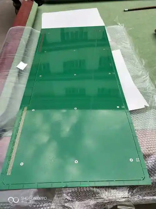
Large - sized circuit board
There is no absolutely unified size standard for "extra - large PCBs". Usually, it is referenced against the maximum general size of conventional PCBs. For PCBs used in ordinary consumer electronics or industrial equipment, most of their sizes are within "length 500mm × width 400mm". However, the sizes of extra - large PCBs generally exceed this range. Common specifications can reach a length of 1000mm - 2000mm and a width of 600mm - 1200mm. Some customized products can even achieve an ultra - large scale of "length over 3000mm and width over 1500mm"
Get a Quote
I. Emergence of Extra - large PCBs
In the development trends of industrial equipment becoming larger, new energy systems being integrated, and medical instruments achieving higher precision, traditional small - sized PCBs can no longer meet the requirements of "high integration, fewer connections, and strong stability" for complex devices. Thus, extra - large PCBs came into being. It is not simply an enlargement of size but a high - end circuit board that combines special materials, precision processes, and scientific designs. It has become a core component to support the stable operation of large - scale electronic devices and is widely used in key fields such as new energy, industrial control, medical, and aerospace.
II. Definition and Size Range of Extra - large PCBs
There is no absolute unified standard for extra - large PCBs in the industry. Usually, it is referenced based on the general size of ordinary PCBs. For PCBs used in ordinary consumer electronics or small - to - medium - sized industrial equipment, most of their sizes are within a length of 500mm × a width of 400mm. However, the sizes of extra - large PCBs generally exceed this limit. Common specifications are a length of 1000 - 2000mm and a width of 600 - 1200mm. Some customized products can even reach a length of over 3000mm and a width of over 1500mm. It should be noted that "extra - large" needs to be judged comprehensively considering the board thickness and the number of layers. For example, a 24 - layer PCB with a length of 1800mm × a width of 1000mm × a thickness of 6mm has a much higher manufacturing difficulty than a single - layer board of the same size. It belongs to an "extra - large + high - order" composite product, with more stringent requirements for technology.
III. Core Technical Features of Extra - large PCBs
The technical difficulties of extra - large PCBs run through the entire process of design, materials, manufacturing, and testing. The core features are mainly reflected in the following four aspects:
(1) Material Selection: Balancing Stability and Compatibility
The commonly used FR - 4 base material for ordinary PCBs is prone to warping and deformation due to thermal expansion and contraction or mechanical stress in extra - large sizes. Therefore, extra - large PCBs need to select special base materials with high Tg (glass transition temperature) and low CTE (coefficient of thermal expansion). The mainstream choices are high - Tg FR - 4 base materials with Tg ≥ 170℃ or halogen - free high - heat - resistant base materials. In some high - power scenarios such as new - energy inverters, metal - based copper - clad laminates like aluminum - based or copper - based ones are used to enhance heat dissipation. At the same time, key material indicators need to be strictly controlled. The CTE needs to be controlled within ≤ 14ppm/℃ on the X/Y axis (about 16 - 18ppm/℃ for ordinary FR - 4), ensuring minimal dimensional changes during soldering and use to avoid component detachment or circuit breakage. In addition, the prepreg needs to have consistent thermal and dielectric properties with the base material, and the solder - resist ink needs to have high adhesion and anti - yellowing properties to prevent coating cracking during long - term use.
(2) Manufacturing Process: Breaking through the Precision Bottleneck
The manufacturing process of extra - large PCBs is the same as that of ordinary PCBs, but each step needs to solve the precision deviation problems caused by the large size. For base - material cutting, a CNC large - scale cutting machine is required, with the error controlled within ±0.1mm (±0.2mm for ordinary PCBs) to avoid inter - layer misalignment in subsequent lamination. Lamination uses a multi - stage vacuum laminator, which applies uniform pressure (pressure ≥ 30kg/cm²) and slowly heats up (heating rate ≤ 2℃/min) to prevent bubbles and delamination. Drilling uses a large - scale CNC drilling machine equipped with an automatic positioning and calibration system to ensure that the drilling position deviation between the edge and the center of the board is ≤ 0.05mm (≤ 0.1mm for ordinary PCBs), and the hole - wall roughness of deep holes is ≤ 25μm to reduce signal transmission loss. For contour machining, a composite process of CNC milling + laser cutting is used, and 3D scanning is required for real - time calibration of irregularly shaped boards to ensure that the profile tolerance is ≤ ±0.15mm.
(3) Structural Design: Balancing Integration and Stress
Extra - large PCBs often integrate multiple modules and high - power components. During the design, it is necessary to balance functional integration and stress dispersion. In terms of stress dispersion, ribs or rounded - corner structures are added at the edges of the board and in component - intensive areas to avoid bending due to gravity during handling and installation. For boards weighing over 5kg, lifting holes or support points are reserved to prevent fatigue deformation during long - term use. In terms of zoned layout, high - power modules (such as power circuits) are separated from weak - signal modules (such as control circuits), and a copper - foil isolation layer and other shielding strips are set in the middle to reduce electromagnetic interference. At the same time, a heat - dissipation via array (hole diameter 0.3 - 0.5mm, hole pitch 1 - 2mm) is designed under high - power components to improve heat - dissipation efficiency. In wiring optimization, for signal lines over 500mm, serpentine wiring or impedance - matching design is used to control the characteristic impedance deviation within ≤ ±10% to avoid signal reflection or delay.
(4) Performance Stability: Meeting Long - term Reliability Requirements
The application scenarios of extra - large PCBs are mostly long - term continuous operation or harsh environments, with extremely high requirements for performance stability. In terms of heat resistance, it needs to pass a temperature - cycle test of - 40℃ ~ 125℃ for 1000 cycles without delamination, cracking, or component detachment at solder joints. In terms of mechanical strength, the flexural strength should be ≥ 450MPa (about 350MPa for ordinary FR - 4), and the impact resistance needs to pass a 1 - kg steel - ball drop test from a height of 1m without damage. For outdoor - application boards, they need to pass a 48 - hour salt - spray test with a 5% NaCl solution and a 1000 - hour ultraviolet - aging test without surface corrosion or coating peeling.
IV. Application Fields of Extra - large PCBs
(1) New Energy Field
Large - scale photovoltaic inverters (power ≥ 100kW) and energy - storage converters (PCS) need to integrate multiple IGBT modules, filter circuits, and control units. The traditional solution uses multiple PCBs connected by wires, which is prone to poor contact. However, a 16 - layer extra - large PCB with a length of 1200mm × a width of 800mm can integrate all modules, reducing the number of wires and improving system reliability. It requires high heat resistance (Tg ≥ 180℃), high heat - dissipation, and high voltage resistance (insulation resistance ≥ 10¹²Ω).
(2) Industrial Control Field
Industrial robot controllers (multi - axis 联动) and production - line PLC main control boards need to integrate multiple servo - drive modules, sensor interfaces, and communication modules. Extra - large PCBs can integrate control, drive, and communication functions, simplify the internal structure of the equipment, and reduce the failure rate. It requires high - precision wiring (line width /line - spacing ≥ 0.1mm/0.1mm) and low electromagnetic interference (passing the EMC test with radiated emission ≤ 54dBμV/m).
(3) Medical Equipment Field
The signal - processing units of CT machines and magnetic resonance imaging (MRI) need to integrate multi - channel signal acquisition and data - operation modules. Extra - large PCBs enable seamless signal transmission from acquisition to operation, reducing signal loss and improving diagnostic accuracy. It requires low dielectric loss (tangent of dielectric loss angle ≤ 0.002) and high cleanliness (manufactured in a class - 1000 clean room).
V. Advantages and Challenges of Extra - large PCBs
(1) Advantages
First, it simplifies the system structure. Integrating multiple modules on one board instead of splicing multiple boards reduces connectors and wires, reducing the risks of poor contact and signal interference. Second, it improves space utilization. Optimizing the internal layout of large - scale equipment reduces the equipment volume. For example, the volume of a certain photovoltaic inverter is reduced by 20% after using an extra - large PCB. Third, it reduces costs and cycle times. Reducing the procurement and assembly of connection components also reduces the later maintenance cost. For example, the failure rate of a certain production - line main control board is reduced from 5% to 0.5%.
(2) Challenges
The manufacturing difficulty is high. Special large - scale equipment is required, with an investment cost 3 - 5 times that of an ordinary PCB production line. The process parameters are strictly controlled, and the yield rate (80 - 90%) is lower than that of ordinary PCBs (about 95%). Transportation and installation are inconvenient. Large - sized boards (such as length 2000mm × width 1000mm) weigh 10 - 20kg, requiring customized anti - static transport racks, and special tools are needed for installation, increasing logistics and construction costs. The design threshold is high. It requires knowledge from multiple disciplines such as structural mechanics, thermal design, and electromagnetic compatibility. The design cycle (3 - 6 weeks) is 2 - 3 times that of ordinary PCBs (1 - 2 weeks).


