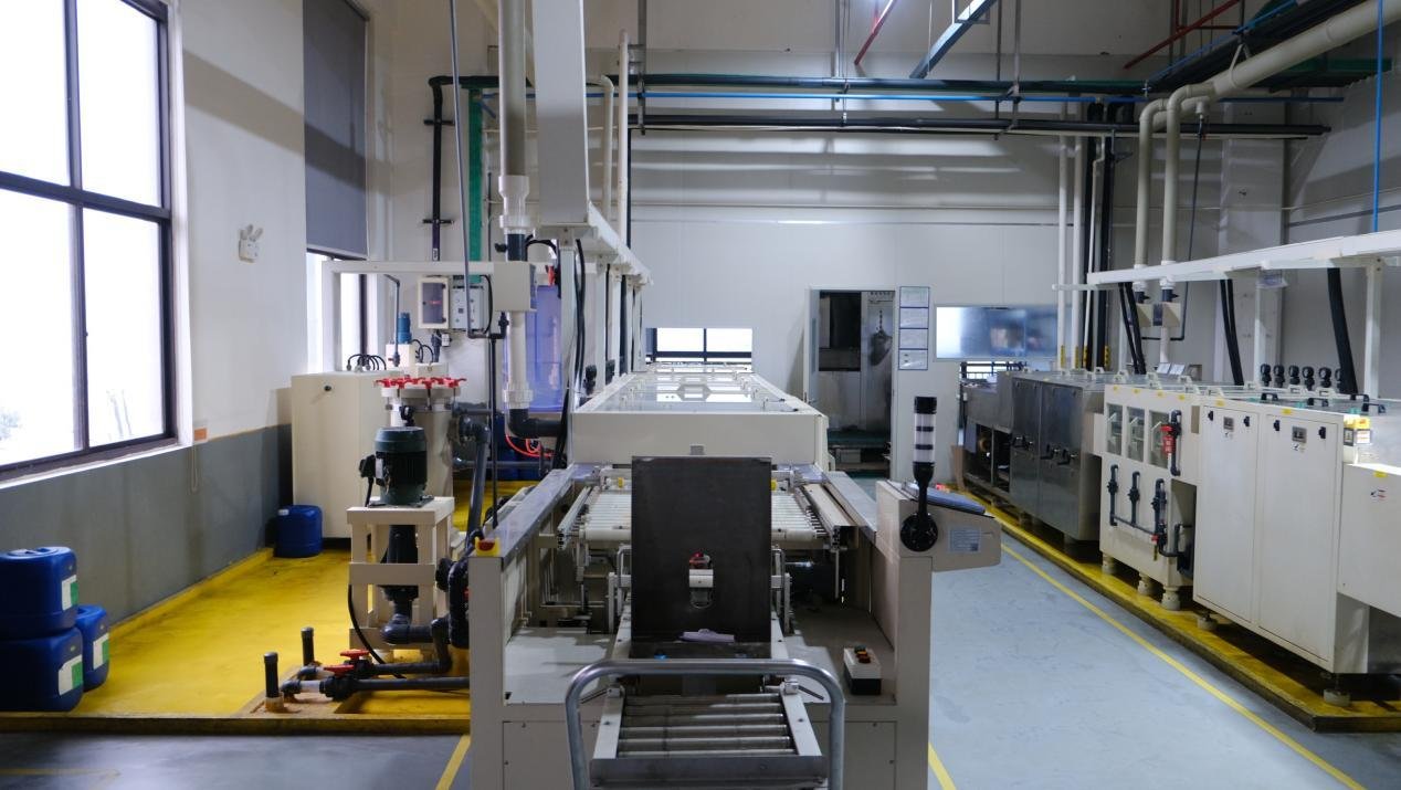
HASL Line
ASL (Hot Air Solder Leveling) is one of the core technologies in the surface coating process of PCB (Printed Circuit Board) manufacturing. Its main function is to form a uniform solder layer on the surface of the PCB copper foil, providing good solderability, electrical conductivity, and anti - oxidation protection for subsequent component soldering (such as SMT pasting, through - hole insertion)
Get a Quote
I. Core Logic of HASL
The essence of HASL is to let the exposed copper surface of the PCB be fully infiltrated with solder first (forming an alloy layer), and then "scrape off" the excess solder through high - pressure hot air, finally leaving a uniform and flat solder coating.
Simply put, the process can be summarized as "solder dipping - solder scraping - cooling". The core goal is to solve the problem of "decreased solderability due to easy oxidation of copper" - isolating copper from air through the solder layer (mainly composed of Sn - Pb or lead - free Sn - Cu - Ag alloys, etc.), while ensuring that the solder can fuse well with the PCB surface during soldering.
Simply put, the process can be summarized as "solder dipping - solder scraping - cooling". The core goal is to solve the problem of "decreased solderability due to easy oxidation of copper" - isolating copper from air through the solder layer (mainly composed of Sn - Pb or lead - free Sn - Cu - Ag alloys, etc.), while ensuring that the solder can fuse well with the PCB surface during soldering.
II. Key Steps and Principles of HASL
The HASL process goes through four core steps: "pretreatment → solder dipping → hot - air leveling → cooling". The principles of each step directly determine the final coating quality, as follows:
| Process Step | Core Operation | Principle and Function |
|---|---|---|
| 1. Pretreatment (Crucial Pre - treatment) | Degreasing → Micro - etching → Pickling → Flux Coating | - Degreasing: Clean the oil stains and fingerprints on the PCB surface with alkaline/solvent to prevent oil from hindering solder infiltration. - Micro - etching: Slightly corrode the copper surface with an acidic solution (such as ammonium persulfate) to remove the oxide layer and form a rough microstructure (increasing the specific surface area), enhancing solder adhesion. - Pickling: Neutralize the remaining alkaline substances from micro - etching to prevent subsequent contamination of the solder bath. - Flux Coating: Spray rosin - based flux (main components: resin, activator, solvent). The activator can further remove the remaining oxide layer on the copper surface, the resin forms a protective film to prevent secondary oxidation of copper, and at the same time reduces the surface tension of the solder to help the solder spread evenly. |
| 2. Solder Dipping (Foundation for Solder Layer Formation) | The PCB enters the molten solder bath vertically/horizontally (temperature 240 - 260℃, higher for lead - free solder) and stays for a few seconds | - Infiltration and Alloying: Under the action of the flux, the molten solder (such as Sn - Pb alloy) reacts with the copper foil surface of the PCB to form a thin Cu₆Sn₅ alloy layer (IMC, intermetallic compound) - this alloy layer is the "bridge" between the solder and copper, directly determining the adhesion of the coating (if the IMC is too thin, the solder is easy to fall off; if it is too thick, it will embrittle, affecting reliability). - Solder Spreading: Due to the reduced surface tension of the molten solder, it evenly covers the copper foil surface (including the inner wall of the through - hole), forming the initial solder layer. |
| 3. Hot - air Leveling (Determining Coating Smoothness) | After the PCB is drawn out from the solder bath, it immediately passes through two sets of high - pressure hot - air nozzles (symmetrically upper and lower), with controllable hot - air pressure/temperature | - Scraping off Excess Solder: High - pressure hot air (temperature slightly higher than the solder melting point, about 260 - 280℃) blows onto the PCB surface, blowing away "the excess solder except in the low - lying areas" - for example, the excess solder at the edges of PCB wires and pads is removed, finally leaving a solder layer with uniform thickness (usually 5 - 20μm) and a flat surface. - Through - hole Hole - leveling: The hot air also acts on the through - holes of the PCB, blowing out the excess solder in the through - holes to ensure the through - holes are unobstructed (preventing pin insertion problems in subsequent component insertion). |
| 4. Cooling and Post - treatment | After passing through the hot - air zone, the PCB immediately enters the cooling zone (air - cooled or water - cooled), and then the residual flux is cleaned | - Rapid Cooling: The solder solidifies quickly after cooling, fixing the flat coating shape (if the cooling is too slow, the solder is likely to flow due to gravity, resulting in an uneven surface). - Flux Cleaning: If the residual flux is not removed, it will corrode the PCB or affect subsequent soldering. It is usually removed by spray cleaning or ultrasonic cleaning. |
III. Core Reaction of HASL: Formation of Intermetallic Compound (IMC)
The most crucial "chemical - metallurgical principle" in HASL is the alloying reaction between copper and tin, which is the fundamental reason why the solder layer can stably adhere to the PCB.
When molten tin (Sn) contacts copper (Cu) at high temperature (240 - 260℃), the following reaction occurs:
Cu + 5Sn → Cu₆Sn₅ (η - phase alloy)
The thickness of this Cu₆Sn₅ alloy layer is usually controlled at 0.5 - 2μm:
If the reaction time is too short (insufficient solder - dipping time), the IMC is too thin, and the bonding force between the solder and copper is weak, resulting in "solder peeling" during subsequent soldering or use.
If the reaction time is too long (too long solder - dipping time) or the temperature is too high, a thicker Cu₃Sn (ε - phase alloy) will be further formed. Cu₃Sn is brittle and hard, which will cause the overall embrittlement of the solder layer, and it is prone to cracking under external force.
Therefore, in the HASL process, the solder - dipping temperature and time need to be strictly controlled to balance the thickness and performance of the IMC.
IV. Characteristics and Limitations of HASL (Extension of Principles)
From the principles, the core advantages and disadvantages of HASL can be deduced:
Advantages: Mature process, low cost, good solderability of the solder layer, and can cover through - holes (preferred for through - hole PCBs).
Limitations:
Advantages: Mature process, low cost, good solderability of the solder layer, and can cover through - holes (preferred for through - hole PCBs).
Limitations:
- Hot - air leveling relies on "gravity + hot air", which has poor compatibility with fine - pitch pads (such as SMT pads below 0.4mm) - it is likely to cause solder deficiency or bridging at the pad edges.
- Lead - free HASL (such as Sn - Cu - Ag alloy) has a higher melting point (about 250 - 270℃), requiring higher heat resistance of the PCB substrate (such as FR - 4).
- The coating smoothness is not as good as processes like ENIG (electroless nickel immersion gold), so it is gradually being replaced in high - precision PCBs (such as mobile phone motherboards, chip carriers).


