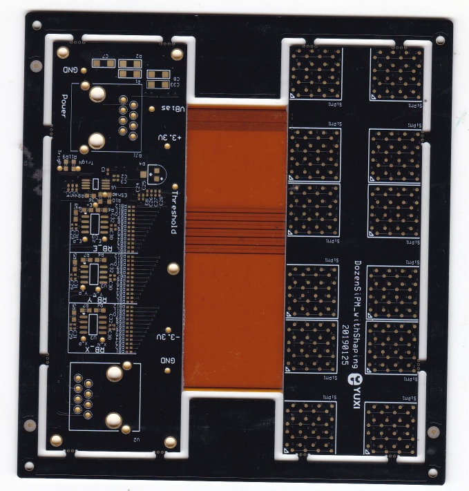
10 layer Rigid-Flex PCB
A 10 - layer rigid - flex PCB usually adopts an alternating "rigid - flexible - rigid" lamination structure, such as 4R + 2F + 4R (where R represents a rigid layer and F represents a flexible layer) or similar combinations. Can you tell me some possible advantages of this "4R + 2F + 4R" structure? Try to express it in English. This will help you practice English and understand the characteristics of 10 - layer rigid - flex PCBs
Get a Quote
Introduction to the Process of 10 - layer Rigid - Flex PCBs
As a high - density and high - reliability circuit - board product, the 10 - layer rigid - flex PCB combines the structural stability of rigid PCBs and the spatial adaptability of flexible FPCs. Its manufacturing process is complex and requires extremely high precision, material compatibility, and reliability control. It is widely used in high - end fields such as foldable - screen terminals, automotive ADAS systems, and medical imaging equipment. The following is a detailed analysis of its production process from three aspects: the core process steps, key technical difficulties, and quality - control system.
I. Core Process Steps: Full - process Control from Design to Finished Product
The production of 10 - layer rigid - flex PCBs needs to take into account the process differences between the rigid and flexible layers. The core process is divided into four major stages: pre - design planning, segmented manufacturing (rigid part + flexible part), rigid - flexible lamination integration, and post - processing. Each step requires strict parameter matching to ensure the final performance.
(1) Pre - design and CAM Engineering Processing
The design stage needs to overcome the dual challenges of "rigid - flexible structure coordination" and "multi - layer signal interconnection", which is the basis for subsequent processes. First, hardware engineers need to determine the 10 - layer lamination structure according to product requirements. The mainstream schemes are "4R + 2F + 4R" (R = rigid layer, F = flexible layer) or "5R + 1F + 4R". The flexible layer should avoid high - frequency signal lines to prevent signal attenuation during bending. The rigid layer needs to plan component layout and heat - dissipation paths and reserve positions for HDI blind and buried vias. Subsequently, CAM engineers carry out data conversion, focusing on three tasks: First, optimize the line width and dielectric - layer thickness through impedance simulation software (such as Ansys SIwave), and control the characteristic impedance within ±10% of the error range of 50Ω (signal lines) or 75Ω (RF lines). Second, design a "stepped" rigid - flexible transition area, and round the edges of the copper foil at the rigid - flexible junction (radius ≥ 0.2mm) to avoid stress concentration. Third, generate CNC files for laser drilling and exposure, and mark the range of the PI protective film to be covered in the flexible area.
(2) Segmented Manufacturing: Independent Processing of Rigid and Flexible Substrates
Due to the large differences in material properties between the rigid layer (with FR - 4 as the base material) and the flexible layer (with PI as the base material), the basic processing needs to be completed on the PCB production line and the FPC production line respectively.
- Rigid - layer Processing: Use 0.2mm - thick FR - 4 copper - clad laminates. The process includes "CNC milling → drilling (hole diameter 0.3 - 0.5mm) → electroless copper plating (copper thickness 0.5μm) → electro - plating copper (total copper thickness 18 - 35μm) → dry - film exposure and development → circuit etching". This forms 4 - 5 independent rigid circuit layers. Each layer needs to be inspected by AOI (Automated Optical Inspection) to check for open - circuits, short - circuits, line - width deviations, etc., and the qualification rate should reach over 99.5%.
- Flexible - layer Processing: Select 12.5μm - thick PI copper - clad laminates (rolled copper foil with an elongation rate ≥ 15% to meet bending requirements). The process should reduce high - temperature steps to avoid deformation of the PI base material. First, achieve inter - layer interconnection through "laser drilling (micro - hole diameter 50 - 100μm) → plasma cleaning of the hole wall → electroless nickel - gold plating (nickel thickness 5μm, gold thickness 0.8μm)". Then, use "semi - cured PI film (adhesive) lamination → low - temperature lamination (180℃, pressure 30kg/cm²)" to form 2 flexible circuit layers. Finally, cover a 25μm - thick PI protective film (the covered area needs to precisely match the rigid - layer lamination area), and verify the adhesion of the protective film through a tensile test (peel strength ≥ 0.8N/mm).
(3) Rigid - Flexible Lamination: Achieving the Integration of the 10 - layer Structure
Lamination is the core process of 10 - layer rigid - flex PCBs, and the key problem of "mismatch of thermal expansion coefficients of different materials" needs to be solved. First, perform "stacking layout" in a clean room (Class 1000): Stack the rigid layers, flexible layers, and prepregs (PP, used as the bonding layer with a thickness of 0.1mm) alternately in the designed order. A "glass - cloth reinforcing sheet" (thickness 0.1mm) should be placed in the rigid - flexible transition area to enhance the mechanical strength of the joint. Then, send it to a vacuum laminator and adopt a "step - by - step temperature - increasing" process: from 80℃ (pre - heating for 30min to exhaust air) → 150℃ (holding for 60min, PP softens and flows) → 200℃ (holding for 90min, PP cures), with the pressure controlled at 25 - 30kg/cm² and the vacuum degree ≤ 10Pa throughout the process to avoid bubbles after lamination. After lamination, it needs to be cooled to room temperature (cooling rate ≤ 5℃/min) to prevent internal stress caused by temperature differences.
(4) Post - processing: Final Formation of Function and Shape
The laminated 10 - layer substrate needs to go through multiple fine processes to be made practical. The first step is "laser drilling and via metallization": To meet the high - density interconnection requirements, use UV laser to drill 0.1 - 0.2mm blind and buried holes in the rigid layer. Through "plasma desmear → electroless copper plating → electro - plating copper", increase the copper thickness on the hole wall to 20μm to achieve vertical interconnection of the 10 - layer circuits. The second step is "surface treatment": Use gold - plating (gold thickness 1 - 3μm, suitable for SMT soldering) in the rigid area and tin - plating (tin thickness 5 - 8μm, to avoid coating cracking during bending) in the flexible area. The third step is "shape processing": Achieve precise forming through "CNC punching (in the rigid area)+ laser cutting (in the flexible area)". The cutting tolerance in the flexible area needs to be controlled within ±0.05mm to prevent edge burrs from affecting the bending performance. Finally, conduct "final inspection", including X - Ray inspection (to verify the quality of via metallization), ICT (in - circuit test to check circuit connectivity), and bending test (the flexible area needs to withstand 180° repeated bending 1000 times without breakage).
II. Key Technical Difficulties: Breaking through the Synergy Bottleneck of Materials and Processes
The process complexity of 10 - layer rigid - flex PCBs is much higher than that of ordinary PCBs. The core difficulties are concentrated in three aspects: inter - layer alignment accuracy, rigid - flexible bonding reliability, and high - density interconnection implementation, which need to be overcome one by one through technological innovation.
(1) Control of Inter - layer Alignment Accuracy: Strict Control of Micron - level Errors
The 10 - layer structure involves multiple laminations, and inter - layer alignment deviation can directly lead to circuit short - circuits or open - circuits. The industry usually adopts a "dual - positioning system" to solve this problem: First, design "optical positioning targets" (circular copper pads with a diameter of 0.5mm) at the edge of each layer of the substrate. Before lamination, the CCD camera automatically identifies the targets to correct the alignment error within ±25μm. Second, adopt "rigid - layer reference positioning", using the outermost rigid layer as a fixed reference. The flexible layer is adapted to the slight deformation during lamination through a "floating fixture" to avoid alignment offset caused by the thermal expansion of the PI base material (thermal expansion coefficient of about 20ppm/℃). In addition, the lamination equipment needs to be equipped with a "real - time pressure monitoring system" to ensure uniform pressure in each area (deviation ≤ 5%) and prevent local substrate deformation from affecting alignment.
(2) Guarantee of Reliability at the Rigid - Flexible Junction: Resisting Stress and Environmental Influences
The rigid - flexible junction is the "weak link" of the product, and it is prone to cracking and delamination due to bending, high temperature, and humidity. The process needs to be optimized in three aspects: First, in material selection, use "modified epoxy PP" as the bonding layer, with a glass - transition temperature (Tg) ≥ 180℃ and a bonding strength with the PI base material ≥ 1.2N/mm, suitable for high - and low - temperature cycling environments (-40℃ to 125℃). Second, in structural design, "gradually thin" the copper foil at the rigid - flexible junction (transition from 35μm to 18μm) to reduce stress concentration caused by sudden changes in material thickness. Third, in reliability testing, 10% of the samples in each batch are selected for "thermal shock testing" (-40℃/30min and 125℃/30min for 100 cycles) and "damp - heat testing" (placed in an 85℃/85% RH environment for 500h). After the test, observe whether there is delamination at the junction through metallographic sectioning, and the qualification rate should reach 100%.
(3) Implementation of High - density Interconnection: Adapting to Small Apertures and Fine Line Widths
The 10 - layer structure needs to support more signal channels, and traditional drilling and etching processes are difficult to meet the requirements. Technically, a combination of "HDI + Laser - direct Imaging (LDI)" is adopted: The HDI process realizes multi - layer interconnection through "laser blind and buried holes + lamination", with the aperture reduced to 50μm and the hole density increased to 200 holes/cm². The LDI technology uses ultraviolet laser to directly expose the circuit on the dry film, with the minimum line - width and line - spacing reaching 30μm/30μm, which improves the accuracy by 50% compared with traditional exposure. In addition, to reduce signal crosstalk, a "ground shielding layer" should be designed between adjacent signal layers, and "differential - pair wiring" (line - spacing is 1.5 - 2 times the line - width) should be adopted. Verify through signal simulation that the crosstalk value ≤ - 30dB to meet the transmission requirements of high - speed signals (such as USB 3.2, PCIe 4.0).
III. Quality - control System: Standardized Management of the Whole Process
The production of 10 - layer rigid - flex PCBs needs to establish a whole - process quality - control system covering "raw materials - processes - finished products" to ensure product stability. In the raw - material stage, FR - 4 base materials need to meet the IPC - 4101 standard, PI base materials need to pass the temperature - resistance test (no deformation at a soldering temperature of 260℃), and copper foils need to be tested for mechanical properties such as elongation and tensile strength. In the process stage, "First Article Inspection (FAI)" should be set after each process. For example, after lamination, the first article needs to be inspected by X - Ray to check the inter - layer bonding state, and after drilling, the first article needs to be tested for hole diameter and hole - wall roughness (Ra ≤ 1.5μm). In the finished - product stage, in addition to conventional electrical - performance testing and appearance inspection, "mechanical reliability testing" (such as bending test, vibration test) and "environmental reliability testing" (such as salt - spray test, high - temperature storage test) also need to be carried out. The final qualification rate of finished products should be controlled above 95% to meet the usage requirements of high - end electronic equipment.