4 layer Flex – rigid PCB
Flexible Layers: Comprise 2 independent PI substrates (both with a thickness of 0.025mm), located respectively between the "top - layer rigid area and the middle rigid sub - layer" and between the "middle rigid sub - layer and the bottom - layer rigid area", forming two independent bending regions.Middle Rigid Sub - layer: Utilizes an ultra - thin FR - 4 substrate (with a thickness of 0.1 - 0.2mm), which is only used to separate the two flexible substrates and arrange the middle - layer circuits (such as the ground layer and shielding layer), without undertaking the main support function.Interconnection Method: Connects the middle rigid sub - layer and the flexible layers through "buried vias", and connects the surface - layer rigid areas and the flexible layers through "blind vias", avoiding through - holes passing through the flexible areas and affecting bending.
Get a Quote
I. Core Structural Framework of 4 - layer Rigid - Flex PCB
The structural design of a 4 - layer rigid - flex PCB needs to balance the "stability of the rigid areas" and the "bendability of the flexible areas". The typical structure takes "rigid area - transition area - flexible area - transition area - rigid area" as the overall framework, and each area realizes functional differentiation through specific layer - stacking combinations. According to the number and position of flexible substrates, the mainstream 4 - layer stacking schemes can be divided into two types: the "2 rigid + 1 flexible" symmetrical structure and the "2 rigid + 2 flexible" composite structure. The specific layer - stacking breakdown is as follows:
(1) Main Stacking Scheme 1: "2 rigid + 1 flexible" Symmetrical Structure (Most Commonly Used)
This scheme takes "rigid substrate + flexible substrate + rigid substrate" as the symmetrical core, with the flexible area in the middle and the rigid areas on both sides symmetrically distributed. It takes into account both structural stability and bending reliability, and is suitable for scenarios where "both ends are fixed and the middle is bent" (such as the hinge circuit of a foldable - screen mobile phone). The specific layer - stacking (from the top layer to the bottom layer) is as follows:
| Layer Number | Area Attribute | Material / Structure Type | Thickness Range | Core Function |
|---|---|---|---|---|
| 1 | Top - layer Rigid Area | Rigid substrate (FR - 4) + copper - foil circuit | Substrate: 0.2 - 0.4mm | ① Bears top - layer components (such as chips, connectors) and provides mechanical support. ② Arranges high - frequency / high - power circuits to ensure signal integrity. |
| 2 | Transition Area → Flexible Area | Flexible substrate (PI polyimide) + copper - foil circuit | Substrate: 0.025 - 0.05mm | ① Core of the flexible area: Enables the bending transmission of circuits. The PI substrate can withstand more than 100,000 bending times (180° bending). ② Transition area: Reduces stress concentration through a gradually changing thickness (from rigid substrate to prepreg to flexible substrate), avoiding inter - layer cracking during bending. |
| 3 | Bottom - layer Rigid Area | Rigid substrate (FR - 4) + copper - foil circuit | Substrate: 0.2 - 0.4mm | ① Bears bottom - layer components (such as resistors, capacitors), forming a symmetrical support with the top - layer rigid area. ② Arranges power / ground circuits, forming a "signal - ground" reference structure with the top - layer signal circuits to reduce interference. |
| 4 | Inter - layer Connection | Metallized vias (through - holes / blind vias) + prepreg (PP) | Via diameter: 0.1 - 0.2mm | ① Metallized vias: Realize the electrical connection of the 4 - layer circuits (through - holes penetrate the entire board, and blind vias connect the surface layer of the rigid area and the inner layer of the flexible area). ② Prepreg: Only used in the rigid area and the transition area to bond the rigid substrate and the flexible substrate. There is no prepreg in the flexible area (to avoid affecting bending). |
Key design details: The flexible area only retains "PI substrate + copper - foil circuit", without a rigid substrate and prepreg. The copper - foil circuit adopts an "arc - corner" design (to avoid stress concentration at right - angles). The prepreg in the transition area should be a "low - fluidity resin" to prevent resin from overflowing into the flexible area during lamination, affecting the bending performance.
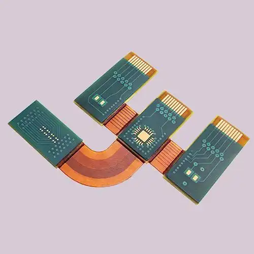
(2) Main Stacking Scheme 2: "2 rigid + 2 flexible" Composite Structure (for High - integration Requirements)
Based on the "2 rigid + 1 flexible" structure, this scheme adds one more flexible substrate, forming a composite structure of "rigid area - flexible area - rigid sub - layer - flexible area - rigid area". It is suitable for scenarios with "multiple - area bending and high - circuit density" (such as the multi - joint circuits of minimally invasive medical devices), and can achieve "independent layout of 4 - layer circuits + multi - direction bending". The specific layer - stacking features are as follows:
- Flexible Layers: Comprise 2 independent PI substrates (both with a thickness of 0.025mm), located respectively between the "top - layer rigid area and the middle rigid sub - layer" and between the "middle rigid sub - layer and the bottom - layer rigid area", forming two independent bending regions.
- Middle Rigid Sub - layer: Utilizes an ultra - thin FR - 4 substrate (with a thickness of 0.1 - 0.2mm), which is only used to separate the two flexible substrates and arrange the middle - layer circuits (such as the ground layer and shielding layer), without undertaking the main support function.
- Interconnection Method: Connects the middle rigid sub - layer and the flexible layers through "buried vias", and connects the surface - layer rigid areas and the flexible layers through "blind vias", avoiding through - holes passing through the flexible areas and affecting bending.
II. Core Structural Components: Coordination and Adaptation of Materials and Processes
The structural reliability of a 4 - layer rigid - flex PCB depends on the coordination of "special materials + precise processes". The core components include flexible substrates, rigid substrates, inter - layer bonding materials, and metallized vias. The selection and design of each component directly determine the product performance:
(1) Flexible Substrate (Core of Bendability)
- Core Material: The mainstream is the PI (polyimide) substrate, which has high - temperature resistance (long - term use temperature from - 269℃ to 280℃) and good bendability (more than 100,000 bending times at 180°). In some high - end scenarios, the PEN (polyethylene naphthalate) substrate is used (lower cost, slightly inferior to PI in terms of bendability).
- Thickness Control: The thickness of the flexible substrate is usually 0.025 - 0.05mm (about 1/10 of that of a common FR - 4 substrate). If it is too thick, it will reduce bending flexibility; if too thin, it will affect the circuit - bearing capacity.
- Circuit Design: "Rolled copper foil" is selected for the copper foil (better ductility than electrolytic copper foil, less likely to break during bending). The line width and line spacing should be ≥0.05mm/0.05mm (to avoid fine - line breakage during bending), and large - volume components (such as resistors with a package of ≥0402) are prohibited from being arranged in the flexible area.
(2) Rigid Substrate (Core of Mechanical Support)
- Core Material: Select a high - Tg (glass - transition temperature ≥170℃) FR - 4 substrate to ensure that the rigid area does not deform during soldering (such as 260℃ reflow soldering) and use.
- Thickness Adaptation: The thickness of the rigid substrate is designed according to the support requirements, usually 0.2 - 0.4mm (single piece). If it needs to bear heavy components (such as camera modules), 2 layers of FR - 4 substrates can be stacked (total thickness 0.4 - 0.8mm).
- Component Layout: All large - volume and high - weight components (such as connectors, chips) should be arranged in the rigid area, and the distance from the transition area should be ≥2mm (to avoid stress concentration in the transition area caused by the weight of the components).
(3) Inter - layer Bonding Material (Core of Structural Stability)
- Bonding in Rigid Areas: Use a conventional prepreg (PP, with the same resin composition as FR - 4), with a thickness of 0.05 - 0.1mm to ensure firm bonding between rigid layers without bubbles or delamination.
- Bonding in Transition Areas: Use a "low - fluidity prepreg" (such as Panasonic R - 1515) with a resin fluidity of ≤15% to prevent resin from overflowing into the flexible area during lamination, affecting bending.
- Treatment in Flexible Areas: No prepreg is used in the flexible area. The inter - layer stability is maintained only by the self - bonding force between the copper foil and the PI substrate. Some high - end products will cover a "PI cover film" (with a thickness of 0.025mm) on the surface of the flexible area to enhance circuit protection.
(4) Metallized Vias (Core of Inter - layer Interconnection)
- Via Type Selection: "Through - holes" can be used in the rigid area (penetrating the entire board to connect all layers), while "blind vias / buried vias" must be used in the transition area and the flexible area (to avoid the breakage of the metallized via walls of through - holes during bending).
- Via - wall Treatment: For blind vias in the flexible area, the "laser drilling + electroless copper plating" process should be adopted. The thickness of the copper layer on the via wall should be ≥15μm (to ensure reliable conductivity), and the roughness of the via wall should be ≤1.5μm (to reduce stress concentration during bending).
- Via - diameter Control: The diameter of blind vias in the flexible area should be ≤0.2mm (if the via diameter is too large, the PI substrate is likely to crack during bending), and the diameter of through - holes in the rigid area can be relaxed to 0.3mm (to fit the pins of connectors).
III. Key Principles of Structural Design (Avoiding Common Failures)
The structural design of a 4 - layer rigid - flex PCB needs to avoid three major risks: "bending fracture, inter - layer delamination, and signal interference". The core principles include:
(1) Design Principles for Flexible and Transition Areas
- Bending Radius Control: The minimum bending radius of the flexible area should be ≥3 times the total thickness of the flexible area (for example, if the total thickness of the flexible area is 0.1mm, the minimum bending radius should be ≥0.3mm) to avoid excessive bending causing circuit breakage.
- Transition - area Length Design: The length of the transition area (from the rigid area to the flexible area) should be ≥5mm, and a "gradually changing thickness" design should be adopted (gradually changing from 0.4mm in the rigid area to 0.05mm in the flexible area) to reduce stress concentration.
- Prohibition of Cross - area Wiring: When a circuit enters the flexible area from the rigid area, "line - width transition" should be completed in the transition area (line width in the rigid area is 0.1mm → gradually changes to 0.05mm in the transition area → line width in the flexible area is 0.05mm). It is prohibited for the line width to suddenly change (become wider or narrower) in the flexible area.
(2) Principles of Inter - layer Symmetry and Balance
- Symmetrical Design of Rigid Areas: The thickness of the substrates and copper foils in the top - layer and bottom - layer rigid areas should be exactly the same (for example, the top - layer is FR - 4 0.3mm + 1oz copper, and the bottom - layer has the same specification) to avoid warping of the rigid area due to uneven stress after lamination.
- Circuit Balance in Flexible Areas: The upper and lower - layer circuits in the flexible area should be symmetrically arranged (for example, if 2 signal lines are arranged on the top - layer, 2 ground lines should be arranged at the corresponding position on the bottom - layer) to avoid the offset of the flexible area during bending due to uneven circuit distribution.
(3) Principles of Signal and Power Isolation
- Zoning Layout: In the rigid area, "high - frequency signal circuits" (such as USB 3.0, MIPI) and "high - power power circuits" (such as 5V/2A) should be arranged on different layers (for example, signals on the top - layer and power on the bottom - layer), separated by a ground layer in the middle.
- Shielding in Flexible Areas: If high - frequency signals need to be transmitted in the flexible area (such as the display signal of a foldable - screen mobile phone), a "ground copper - foil layer" can be added in the flexible area (located between two layers of signal lines) to form a "signal - ground - signal" shielding structure, reducing signal interference during bending.


