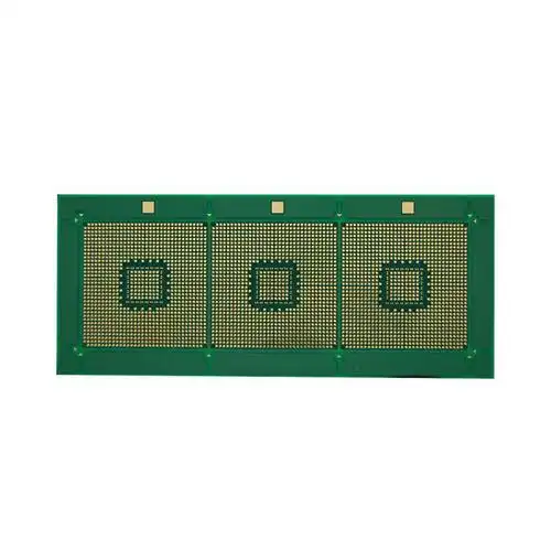
IC Substrate PCB
IC packaging substrate materials have a core system of "base material + copper foil + solder resist". For base materials, BT resin (with a dielectric constant of 3.0 - 3.5 and heat resistance above 260℃) and ABF insulating film (low - loss, suitable for fine lines below 10μm) are commonly used. In high - end scenarios, PI or PTFE is adopted. The copper foil selected is 1/4 - 1/2OZ ultra - thin electrolytic copper (roughness Ra≤0.5μm) to ensure the formation of fine circuits. Photosensitive epoxy resin is used as the solder resist to achieve high - precision window - opening. These materials need to have low signal loss, high thermal conductivity, and thermal shock resistance to meet the requirements of high - density interconnection and reliability in chip packaging
Get a Quote
I. Base - material Pretreatment and Pattern Transfer (Procedures 1 - 3)
- Base - material Cutting and Surface ActivationSelect BT resin copper - clad laminates (core - board thickness of 0.1 - 0.2mm, copper - foil thickness of 1/4OZ/9μm). Cut them to the designed size (such as 150mm×150mm) using a laser cutting machine with an error of ±0.05mm. After cutting, activate the surface with a plasma processor (Ar/O₂ mixed gas), increasing the surface energy of the base material from 30mN/m to 45mN/m to enhance the adhesion of the photosensitive film. Finally, bake at 120℃ for 1 hour to remove moisture, ensuring the water absorption rate is ≤0.03%.
- Photosensitive Film Coating and LDI ExposureCoat an ultra - thin photosensitive film (thickness of 8 - 10μm, suitable for fine - line requirements) by roll - coating at a speed of 0.8m/min. Use a Laser - Direct Imaging (LDI) system to expose with 355nm ultraviolet laser, achieving a resolution of 2μm to form the circuit pattern. After exposure, develop with a 0.8% sodium carbonate solution, controlling the development time at 60±5 seconds to ensure no residual glue at the pattern edges.
- Fine - etching and Film StrippingUse an acidic etchant (copper chloride concentration of 160g/L, temperature of 38℃) and adopt the "low - pressure spray + step - by - step etching" process. The etching rate is 0.6μm/min to etch the 1/4OZ copper foil into inner - layer circuits with a line - width of 5 - 10μm, controlling the under - etching amount to ≤2μm. After etching, strip the film with a 5% sodium hydroxide solution, and then conduct an AOI inspection. Focus on checking for open - circuits, short - circuits, and line - width deviations (required to be ≤±1μm).
II. Inter - layer Interconnection and Stacking Construction (Procedures 4 - 6)
- Micro - blind - hole ProcessingUse a UV laser drilling machine (wavelength of 355nm) to process micro - blind holes. Control the aperture within 20 - 50μm and the hole - position deviation at ±1μm. Before drilling, calibrate the reference holes of the base material through an X - ray positioning system to ensure the micro - blind holes are precisely aligned with the lower - layer circuits. After drilling, treat with a plasma desmear process (O₂/CF₄ volume ratio of 4:1) to remove the resin residue and carbonized layer on the hole wall, with the hole - wall roughness Rz≤5μm.
- Via Metallization and Electro - plating ThickeningFirst, conduct electroless copper plating to deposit a 0.5 - 1μm conductive layer on the hole wall to ensure hole - wall conductivity. Then, use a pulse electro - plating process (frequency of 20kHz, current density of 1A/dm²) to thicken the copper layer on the hole wall to 8 - 12μm, and at the same time, electro - plate and thicken the circuit surface to 15μm. Monitor the plating solution temperature (25±1℃) and pH value (10±0.2) in real - time during electro - plating to avoid uneven copper thickness in the holes.
- Lamination and StackingStack in the order of "BT base material - prepreg (BT resin system) - inner - layer circuit board - prepreg - base material". Select a low - resin - flow prepreg (resin - flow amount ≤ 15%) to ensure the board - thickness deviation after lamination is ±0.01mm. Use a vacuum hot - press for lamination and execute a temperature - control program: 80℃ (10kg/cm², 20min) for exhaust → 150℃ (20kg/cm², 30min) for resin flow → 180℃ (25kg/cm², 60min) for curing. After lamination, detect the inter - layer alignment accuracy through X - ray (deviation ≤ ±2μm).
III. Outer - layer Processing and Packaging Adaptation (Procedures 7 - 10)
- Outer - layer Circuit ManufacturingRepeat the "photosensitive film coating - LDI exposure - etching" process to make the outer - layer circuits with a line - width accuracy of ±1μm. The outer - layer circuits need to be precisely connected to the micro - blind holes. Ensure the alignment deviation is ≤±1.5μm through a CCD vision positioning system. After etching, conduct a second AOI inspection, focusing on checking the connection integrity between the outer - layer circuits and the blind holes.
- Solder - mask Layer Printing and CuringUse screen - printing to coat photosensitive solder - mask ink (thickness of 10 - 15μm). The ink should be compatible with the BT resin base material, and the adhesion after curing should be ≥5B. Open windows for the pad areas through an LDI exposure machine. The window size should be 5 - 10μm larger than the pads to ensure accurate ball - mounting. The curing temperature of the solder - mask layer is 150℃ for 60 minutes to avoid substrate deformation due to high temperature.
- Surface Treatment (UBM Manufacturing)To achieve the welding interconnection between the chip and the carrier board, a Under - Bump Metallization (UBM) layer needs to be made: First, electro - plate nickel (thickness of 5 - 8μm) in the pad area, and then electro - plate gold (thickness of 0.5 - 1μm), or use an electroless nickel - gold process. After surface treatment, detect the coating thickness with a profilometer, with a deviation of ≤±0.5μm to ensure the reliability of ball - mounting.
- Shape Processing and Finished - product InspectionCut the shape of the carrier board with a laser cutting machine with a cutting accuracy of ±0.02mm to avoid edge chipping caused by mechanical cutting. The finished product needs to pass three core inspections: ① Electrical performance (flying - probe test for open - circuits and short - circuits, insulation resistance ≥ 10¹¹Ω); ② High - frequency performance (network analyzer tests the insertion loss in the 10GHz frequency band to be ≤0.5dB/cm); ③ Reliability (-40℃~125℃ temperature cycling for 1000 times, no delamination or hole - copper fracture). After passing, conduct laser marking according to packaging requirements to complete the production of the IC carrier board.


