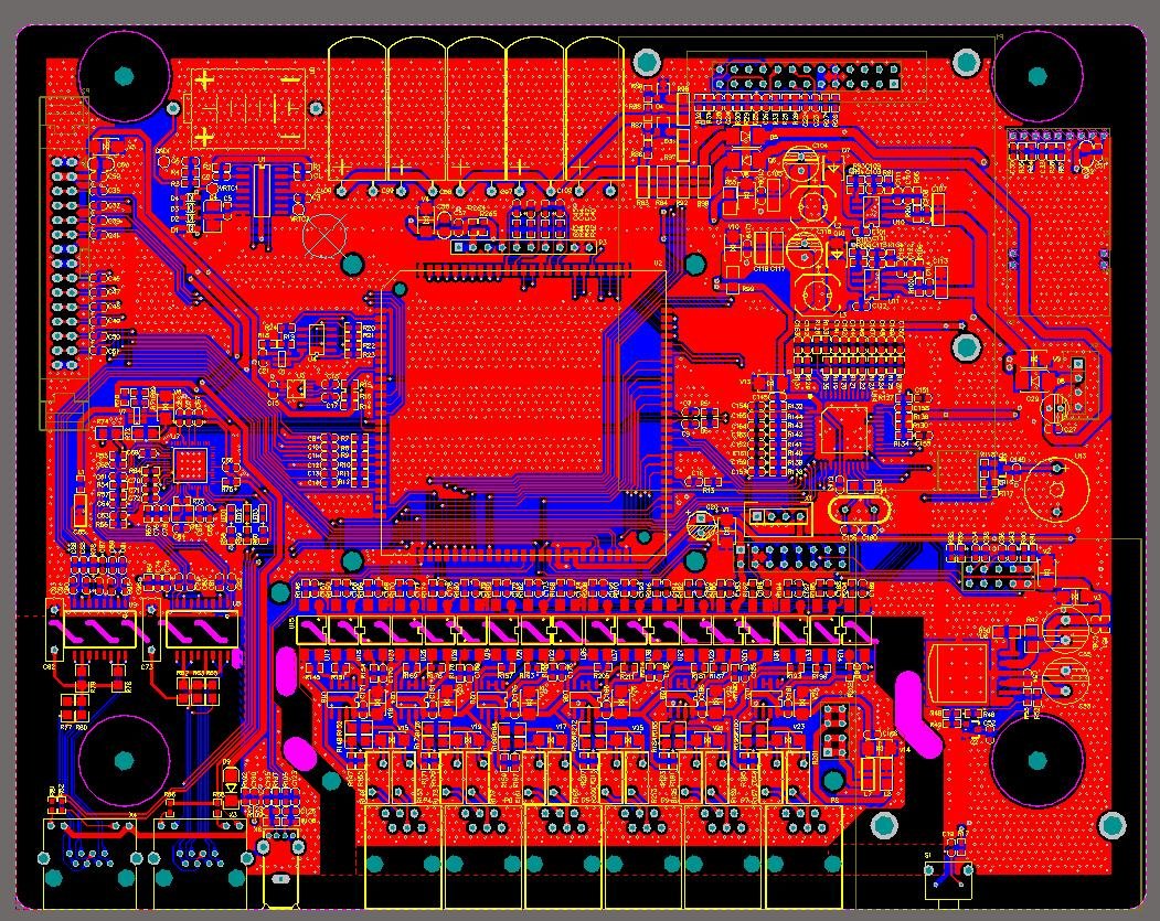
PCB Layout
PCB Layout (Printed Circuit Board Layout and Wiring) is a crucial step in electronic hardware design, bridging the gap between "abstract circuit logic" and "physical PCB products". Based on the netlist generated from the PCB schematic diagram, it completes the physical layout of components, signal line wiring, rule verification, and production file output in professional design software. Eventually, it transforms the electrical connections defined in the schematic diagram into a manufacturable, high - performance, and highly reliable physical substrate. The design quality directly determines the functional stability, signal integrity, electromagnetic compatibility (EMC), and production feasibility of electronic products, and is an important part of the core skill set of hardware engineers.
Get a Quote
PCB Layout: The Core Implementation Link Transforming Electronic Hardware from Logic to Physical Form
I. Core Objectives and Design Constraints of PCB Layout
1. Three Core Objectives
- Functional Fidelity: Strictly follow netlist information to ensure that the pin connections of all components are completely consistent with the schematic, without misconnections, missing connections, or short circuits. This is the basic requirement of Layout. For example, the I/O pins of an MCU must be accurately connected to the signal terminals of sensors, and the output terminal of a power chip must be correctly connected to the power supply terminal of the load. Any connection deviation may lead to circuit function failure.
- Performance Optimization: Develop differentiated routing strategies for different types of signals (power, high-speed, and sensitive signals) to reduce signal loss, interference, and timing deviations. For instance, high-speed DDR memory signals require controlled impedance matching and line length consistency to avoid data transmission errors; analog audio signals need to be isolated from digital noise to ensure pure sound quality; power traces need to reduce impedance to minimize voltage drops and ripples.
- Manufacturing Compatibility: The design must align with PCB manufacturing and Surface Mount Technology (SMT) process capabilities to avoid situations where "the design is feasible but cannot be produced by the factory". For example, the trace width must meet the minimum processing capacity of the factory (≥0.2mm for conventional processes), the component spacing must reserve space for placement errors (≥0.1mm), and via specifications must match the precision of drilling equipment (minimum hole diameter ≥0.3mm). These measures help reduce production defect rates and costs.
2. Three Types of Key Constraints
- Mechanical Constraints: Determined by the product casing and installation scenario, including the length and width dimensions of the PCB, shape (e.g., rectangular, circular, irregular), position and hole diameter of positioning holes (e.g., φ3mm positioning holes with a center distance of 50mm to fit the casing screws), and component height limitations (e.g., the PCB of wearable devices must control component height ≤3mm to avoid exceeding the casing thickness).
- Electrical Constraints: Defined by circuit performance requirements, such as power supply voltage levels (3.3V, 5V, 12V) and maximum current (USB 2.0 interfaces must carry 1A current, corresponding to a trace width ≥0.5mm; motor drive circuits must carry 5A current, with a trace width ≥2mm), high-speed signal impedance (USB3.0 differential pair impedance 90Ω±10%, Ethernet signal impedance 50Ω±10%), and EMC standards (medical equipment must meet EN 60601-1, industrial equipment must meet EN 55032 Class B).
- Process Constraints: Determined by the processing capabilities of the PCB factory, including the number of PCB layers (single/double-layer boards for simple circuits, 4 or more layers for complex high-speed circuits), substrate type (FR-4 epoxy glass cloth substrate for conventional circuits, Rogers RO4350 substrate for high-frequency RF circuits), copper thickness (1oz copper for conventional use, 2oz copper for high-current circuits to reduce line resistance), and minimum trace width/spacing (≥0.2mm for conventional processes, 0.15mm for high-density PCBs).
II. Standardized Process of PCB Layout
1. Preparations: Netlist Import and Rule Presetting
- Netlist Import: Export the netlist file (containing component reference designators, package models, and pin connection relationships) from schematic design software such as Altium Designer or KiCad. After importing it into the PCB design software, the software automatically loads the corresponding component packages to form a "component library to be placed". This step requires focusing on verifying the consistency between packages and schematic symbols to avoid subsequent soldering issues caused by incorrect packages (e.g., mistakenly selecting the 0603 package for a 0805 resistor, which will prevent the component from fitting the pad).
- Rule Presetting: Configure routing rules in advance in the PCB software to reduce repeated adjustments during routing. The core rules include:
- Trace Width Rules: Set according to current magnitude (e.g., 0.3mm trace width for 3.3V/0.5A signals, 1mm trace width for 12V/2A power supplies);
- Spacing Rules: Set according to voltage levels and signal types (≥0.2mm spacing for low-voltage signals, ≥1mm spacing between high-voltage and low-voltage signals to avoid creepage);
- Impedance Rules: Set target impedance for high-speed signals (e.g., 90Ω for USB3.0 differential pairs). The software automatically calculates the trace width and spacing based on the substrate dielectric constant and copper thickness;
- Via Rules: Use vias with φ0.3mm hole diameter and φ0.6mm pad for conventional signals, and vias with hole diameter ≥0.5mm for high-current signals.
2. Component Placement: Determining Routing Difficulty and Performance Foundation
- Functional Zoning: Divide the PCB into physical regions according to the functional modules in the schematic to avoid cross-interference between different modules. Taking a 4-layer IoT PCB as an example, the top layer (Top Layer) is used to place signal processing components such as MCUs and sensors; the bottom layer (Bottom Layer) is for interface components such as USB and antennas; the first inner layer is set as a complete GND (ground) plane; and the second inner layer is a 3.3V power plane. This zoning method can reduce the interference of power noise on sensitive signals and shorten the signal transmission path.
- Core Priority: First fix "non-movable" or "performance-critical" components:
- Non-movable Components: For example, USB connectors must be aligned with the casing opening; a space of ≥2mm must be reserved around positioning holes for screw installation (components must be ≥2mm away from positioning holes);
- High-performance Sensitive Components: For example, the crystal oscillator of an MCU must be close to its XTAL pin (distance ≤5mm) to reduce clock signal transmission loss and external interference; WiFi chips must be close to antenna interfaces to avoid RF signal attenuation;
- High-power Components: For example, DC-DC converters and power resistors must be away from heat-sensitive components such as temperature sensors and MCUs (spacing ≥10mm), and sufficient heat dissipation space must be reserved. Heat-dissipating copper pads can be laid under the components to enhance heat dissipation.
- Detail Optimization: Arrange components of the same type (e.g., resistors, capacitors) in alignment with a grid (e.g., 2.54mm grid) to facilitate SMT placement and visual inspection; ensure component spacing ≥0.1mm to avoid bridging during placement; place noise sources such as crystal oscillators and clock chips away from ADC (Analog-to-Digital Converter) and analog audio circuits, and isolate them with ground copper pads if necessary.
3. Signal Routing: Achieving Connection and Performance Optimization
- High-speed Signals (e.g., USB3.0, DDR4): Use differential routing. The two signal traces must be parallel, of equal length (length difference ≤5mil, 1mil=0.0254mm), and with fixed spacing (e.g., 0.2mm spacing for USB3.0 differential pairs); avoid vias (each additional via increases signal loss by approximately 0.1dB); do not cross the split area of the GND plane to prevent interruption of the signal return path; calculate the trace width based on the target impedance (e.g., for FR-4 substrate with 1oz copper thickness, the trace width for 50Ω impedance is approximately 0.3mm).
- Power Signals: Adopt a combination of "thick trace width + copper pouring". For example, use a 1mm trace width or direct copper pouring for 5V/2A power supplies to reduce line resistance and voltage drop; add a 100nF ceramic filter capacitor near the power pin of each component (distance ≤2mm) to suppress power ripples; route multiple power circuits (e.g., 3.3V, 5V) separately to avoid crossing of traces with different voltage levels and prevent crosstalk.
- Sensitive Signals (e.g., ADC Input, Analog Audio): Use short paths and minimize vias; avoid parallel routing with digital signal traces (if parallel routing is unavoidable, the spacing must be ≥5mm); adopt "single-point grounding" (connect to the GND plane through a via only at one end) to avoid ground loops and interference; lay ground copper pads around the signal traces, with a spacing of ≥0.2mm between the copper pads and the signal traces, and add a via every 2mm to connect the copper pads to the GND plane, forming a shielding layer.
- Ordinary Digital Signals (e.g., GPIO): Ensure the trace width ≥0.2mm to meet process and current requirements; avoid acute-angle routing (use ≥45° angles or arc routing) to reduce signal reflection; keep the trace length as short as possible to avoid signal delay caused by long paths.
4. Rule Verification and File Output
- Rule Verification:
- Design Rule Check (DRC): The software automatically checks for errors such as insufficient trace width, excessive spacing, and unconnected nets. All DRC errors must be corrected before proceeding to the next step;
- Signal Integrity Simulation: Simulate high-speed signals to verify whether signal overshoot, ringing, and timing meet standards. If there are issues, adjust the routing (e.g., add terminal matching resistors);
- 3D Preview: Use the 3D function of the PCB software to check whether the component height exceeds the casing limit (e.g., if the internal height of the casing is 5mm, the maximum component height must be ≤4.5mm) and whether there is mechanical interference (e.g., conflict between the connector and screws);
- Cross-probing: Click on a component or net in the schematic, and the corresponding element in the PCB will be highlighted to verify connection consistency (e.g., whether the PA0 pin of U1 in the schematic is connected to the sensor SDA in the PCB).
- File Output: Export files required for production, including:
- Gerber Files: Contain graphic information of the top layer, bottom layer, power layer, ground plane, solder mask layer, and silkscreen layer. They are the core files for PCB factories to manufacture substrates;
- Drill Files: Mark the hole diameter and coordinates of vias and positioning holes to guide the factory in drilling;
- Bill of Materials (BOM): Include component reference designators, models, parameters, packages, and quantities, which are used for procurement and material management;
- Pick and Place Files: Contain the X/Y coordinates and rotation angles of each component to guide the SMT placement machine in accurately placing components.
III. Key Design Principles and Common Problem Solutions
1. Core Design Principles
- Grounding Optimization: Prioritize "plane grounding" (with a complete GND plane in the inner layer) rather than "trace grounding" to reduce ground impedance; route analog ground (AGND) and digital ground (DGND) separately, and connect them at a single point through a 0Ω resistor or bead only at the power input to avoid digital ground noise interfering with analog signals; use thick trace widths or copper pouring for high-current ground (e.g., power ground PGND), and connect it to the power ground independently without sharing it with signal ground.
- EMC Control: Add common-mode inductors, X-capacitors (across the power line and neutral line), and Y-capacitors (across the power supply and ground) at the power input to suppress common-mode noise; lay ground copper pads around sensitive signals and connect them to ground at multiple points; route clock signals and RF signals on inner layers or wrap them with ground copper pads to reduce electromagnetic radiation; reserve a "ground edge" of ≥5mm around the PCB to enhance EMC performance.
- Process Compatibility: Avoid designing "island copper pads" (isolated copper pads not connected to ground or power, which may fall off during soldering). If they exist, connect them to the ground plane through thin wires; ensure silkscreen characters are legible, with a height ≥0.8mm and width ≥0.2mm, and avoid overlapping with pads; keep the number of vias moderate to prevent reduced PCB strength due to dense arrangement.
2. Common Problems and Solutions
- High-speed Signal Transmission Errors (Packet Loss, Bit Errors): Mostly caused by unequal differential pair lengths, impedance mismatch, or proximity to interference sources. Solution: Use the software's "length matching" function to correct the length difference; recalculate the trace width and spacing to ensure impedance matching; place high-speed traces away from power modules and clock chips, or isolate them with ground copper pads.
- Excessive Power Ripples: Caused by long power traces, filter capacitors being far from components, or high ground impedance. Solution: Shorten the power traces and use copper pouring; add filter capacitors near the power pins of each component, with a distance ≤2mm; ensure the GND plane is complete to reduce ground impedance.
- Short Circuits After PCB Prototyping: Mostly caused by insufficient spacing between power and ground traces, short circuits of via pads, or netlist errors. Solution: Check the DRC to ensure the spacing between power and ground traces ≥0.5mm; review the Gerber files to check for overlapping of via pads with other traces; re-import the netlist to verify the consistency between the schematic and PCB connections.


