AOI Test
PCB AOI (Automatic Optical Inspection) is a core device in PCB production that combines optical imaging with intelligent algorithms to achieve automatic defect identification. Its core principle can be summarized as "optically capture details → algorithmically compare differences → determine defect types". Essentially, it replaces manual inspection with machine vision, addressing the pain points of low - efficiency, poor - precision, and easy - fatigue in manual inspection
Get a Quote
I. Core Process of PCB AOI Testing: Completing Automatic Detection in 4 Steps
The entire process can be divided into four consecutive steps: "image acquisition → image pre - processing → defect identification → result output". All steps are completed in milliseconds to ensure adaptation to the high - speed operation of the PCB production line (usually the detection speed can reach 0.5 - 2 meters per minute).
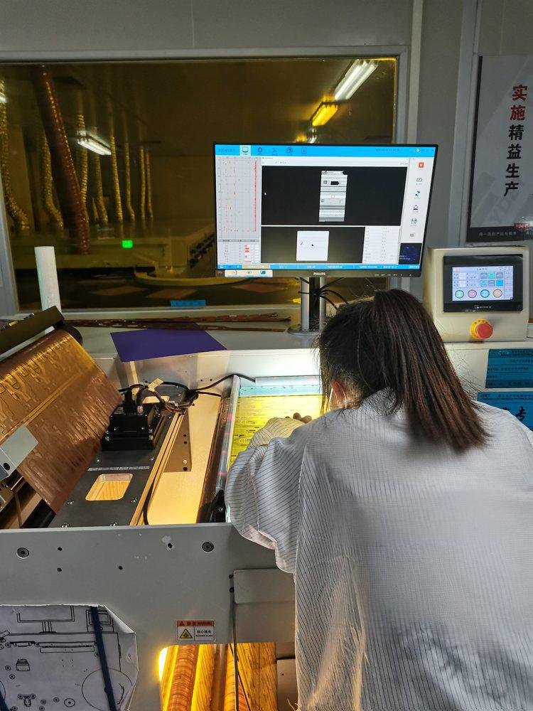
1. Image Acquisition: Capturing PCB Details with "Optical Eyes"
This is the basis of detection. The physical characteristics of the PCB need to be converted into analyzable digital images through an optical system. The core components and their functions are as follows:
Light Source System: It uses multi - angle and multi - spectral light sources (such as red and blue LED lights, and some high - end devices include ultraviolet/infrared light) to solve the problem of reflective interference from different materials on the PCB surface (copper foil, solder resist green oil, silk - screened characters). For example:
Light Source System: It uses multi - angle and multi - spectral light sources (such as red and blue LED lights, and some high - end devices include ultraviolet/infrared light) to solve the problem of reflective interference from different materials on the PCB surface (copper foil, solder resist green oil, silk - screened characters). For example:
- Orthogonal light source (vertical illumination) is used to detect surface flatness (such as solder resist bubbles).
- Oblique light source (45°/60° illumination) is used to highlight edge defects (such as circuit gaps, copper residue).
Optical Lens: It is equipped with high - resolution industrial lenses (usually with a resolution of 5 - 20μm/pixel) to ensure clear capture of tiny details (such as a 0.1mm line - width circuit, 0.2mm aperture).
Industrial Camera: Most use CCD or CMOS cameras to convert optical signals into digital electrical signals, generating 2D grayscale images or 3D height images (some devices support 3D detection for identifying warping, protrusions, etc.).
Motion Control: The conveyor belt drives the PCB to move at a constant speed, and the camera takes continuous photos at fixed intervals (or trigger signals) and stitches them into a complete panoramic image of the PCB.
2. Image Pre - processing: "Optimizing Images" to Reduce Interference
The collected original images may contain noise (such as dust reflection, light source fluctuations), and need to be pre - processed by algorithms to improve image quality for subsequent identification. Common operations include:
- Noise Reduction: "Gaussian filter" and "median filter" are used to eliminate noise points in the image, avoiding misjudgment as tiny defects.
- Gray - scale Correction: To unify the brightness differences in different regions (such as uneven illumination between the edge and the center of the PCB), ensuring that the gray - scale characteristics of the same defect are consistent in the image.
- Image Segmentation: The image is split according to the PCB structure (circuit area, solder - resist area, silk - screen area), and detection parameters are adjusted accordingly (such as focusing on edge detection in the circuit area and character integrity in the silk - screen area).
3. Defect Identification: "Comparison + Analysis" to Find Anomalies
This is the core part of AOI, and defect determination is achieved through two mainstream algorithms:
(1) Template Matching Method (Most Commonly Used, Suitable for Mass - produced Standardized PCBs)
(1) Template Matching Method (Most Commonly Used, Suitable for Mass - produced Standardized PCBs)
- Establishing a Standard Template: First, scan 1 - 3 "qualified PCBs" that have been re - inspected by manual labor to generate a high - precision standard image template, storing feature parameters such as the position, size, and grayscale of circuits, pads, and silk - screening.
- Real - time Image Alignment: Align the coordinates of the image of the PCB to be detected with the standard template (correcting the position deviation caused by conveyor belt offset).
- Pixel - level Comparison: Compare the grayscale values and shape contours of the two pixel by pixel. When the difference in a certain area exceeds the preset threshold (such as a grayscale difference > 30, size deviation > 0.05mm), it is marked as a "suspected defect area".
(2) Feature Extraction Method (Suitable for Non - standard PCBs or Complex Defects)
It does not rely on a standard template, but directly extracts the "typical features" of defects from the image to be detected for determination. For example: - Circuit Defects (Gaps, Short - circuits): Extract the edge continuity feature. If there are breakpoints or abnormal connections in the circuit edge, it is determined as a defect.
- Solder - resist Defects (Bubbles, Exposed Copper): Extract the grayscale mutation feature. If there are local highlights (exposed copper) or dark spots (bubbles) in the solder - resist green - oil area, it is determined as a defect.
- Silk - screen Defects (Missing Printing, Blurring): Extract the character's contour clarity and stroke integrity features. If the character is missing or the edge is blurred, it is determined as a defect.
4. Result Output: Classification, Annotation, and Data Recording
- Defect Classification: The algorithm automatically classifies defects into specific types such as "circuit gap", "solder - resist bubble", "missing silk - screening", "pad offset" according to the shape, position, and grayscale characteristics of the defects.
- Visual Annotation: Mark the defect positions with different - colored boxes on the detection interface and display the defect size (such as "gap length 0.2mm").
- Data Storage: Automatically record the detection results of each PCB (qualified/unqualified, defect type/quantity) and generate reports for production traceability (such as if the solder - resist defect rate of a certain batch of PCBs exceeds the standard, parameters of the solder - resist process can be adjusted by tracing back).
II. Core Technical Advantages of PCB AOI: Solving the Pain Points of Manual Inspection
Compared with manual inspection using magnifying glasses/microscopes, the core advantages of AOI come from its technical characteristics, which are also the key to its popularization in the PCB industry:
- High Detection Efficiency: A single device can detect 1 - 2 PCBs per minute (depending on the board size), 5 - 10 times the efficiency of manual inspection, adapting to mass - production requirements.
- Accurate Detection Precision: It can identify tiny defects as small as 5μm (such as fine copper residue), avoiding missed or misjudgments caused by human fatigue and visual errors.
- Comprehensive Detection Range: It covers the entire PCB production process (inner - layer circuits, outer - layer circuits, solder resist, silk - screening, final product inspection), and can detect more than 20 common defects.
- Data Traceability: Automatically store all detection data and support connection with the MES production system, facilitating the analysis of the root causes of defects (such as quickly locating and adjusting when the defect rate of a certain process increases).
III. Common Detection Defect Types and Identification Logic of PCB AOI
The defect characteristics of PCBs in different processes are different, and AOI will adjust the detection strategy accordingly. The typical ones are as follows:
| Detection Process | Common Defects | AOI Identification Logic |
|---|---|---|
| Inner - layer Circuits | Circuit gaps, short - circuits, line - width deviation, pinholes | Compare the circuit edge contours of the standard template. If there are breakpoints (gaps), abnormal connections (short - circuits), or width deviations exceeding the threshold, it is determined as a defect. |
| Outer - layer Circuits | Pad offset, exposed copper, uneven coating | Use an oblique light source to highlight the pad edges, compare with the standard position coordinates (offset exceeding 0.1mm is determined as a defect); detect uneven coating through grayscale uniformity. |
| Solder - resist Process | Solder - resist bubbles, scratches, missing printing, misalignment | Under the orthogonal light source, bubbles appear as "dark spots" (grayscale lower than the normal area); scratches appear as "bright lines" (reflective differences); compare the solder - resist pattern with the circuit position to determine misalignment. |
| Silk - screen Process | Missing character printing, blurring, wrong printing, offset |


