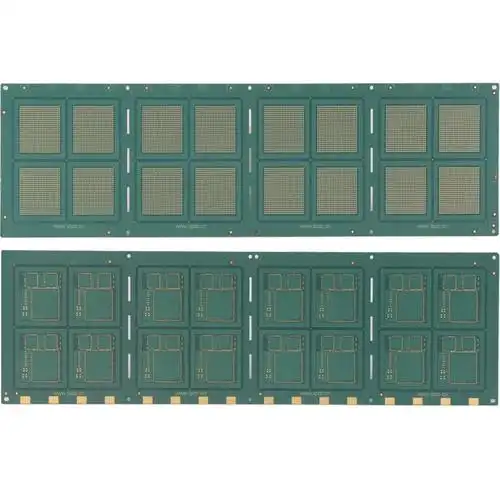
IC package substrate
IC carrier boards (Integrated Circuit Substrates) serve as the "bridge" connecting chips to external circuits and are the core material in high - end packaging. As a crucial carrier in the first - level packaging of integrated circuits, they not only provide mechanical support, circuit protection, and heat conduction for chips, but also achieve high - speed signal transmission between chips and PCBs through high - density wiring. They account for as high as 70% - 80% of the high - end chip packaging cost, being the core link determining the performance, miniaturization, and reliability of electronic devices.
Get a Quote
I. Core Positioning: The Crucial "Linking" Carrier in Chip Packaging
IC carrier boards are the core base materials in the first - level packaging of integrated circuits. Essentially, they are high - end circuit boards upgraded based on HDI boards, undertaking three core functions. First, electrical connection: They connect the tiny pads of chips to the larger interfaces of PCBs through micro - fine - width circuits, enabling precise transmission of signals and power. Second, physical protection: They provide mechanical support for fragile bare chips, isolate environmental interferences such as moisture and dust, and relieve stress impacts during packaging and use. Third, performance optimization: They assist chips in heat dissipation through special materials and structural designs, and some high - end products can also embed passive components to achieve system - function integration. In the packaging cost structure, IC carrier boards play a central role. They account for 40 - 50% of the material cost in low - end wire - bonding (WB) packaging, and as high as 70 - 80% in high - end flip - chip (FC) packaging, making them the most valuable base materials in the semiconductor packaging process. Compared with traditional lead frames, IC carrier boards break through the limitation of the number of pins. The line width and line spacing can be reduced to 8μm (only 1/10 of the diameter of a human hair), and the number of layers can reach more than 22, perfectly adapting to the high - density interconnection requirements of highly integrated chips.
II. Classification System: Dual Dimensions of Materials and Packaging Processes
The classification of IC carrier boards needs to consider material characteristics and packaging requirements, with different types corresponding to differentiated application scenarios.
(1) Classification by Material Characteristics
- Rigid Substrates: This is the mainstream technological direction and can be further divided into three categories. Products based on BT resin as the base material have high heat resistance and low dielectric loss, and are widely used in the packaging of memory chips and RF chips. ABF resin substrates are renowned for their ultra - thin characteristics and high adhesion, and are the core choice for high - end computing chips such as CPUs and GPUs. The value of ABF carrier boards required for a single high - end GPU package is 5 - 8 times higher than that of ordinary chips. MIS resin substrates, with their fine - wiring capabilities, are suitable for the fields of analog and power chips.
- Flexible Substrates: With PI (polyimide) as the core material, they have the advantages of being thin, light, and foldable. They are mostly used in flexible displays and wearable devices in consumer electronics, but have the problem of difficult warpage control.
- Ceramic Substrates: Represented by alumina and aluminum nitride, they have excellent thermal conductivity and insulation, and are suitable for extreme environments such as aerospace and automotive electronics. However, their high cost limits large - scale applications.
(2) Classification by Packaging Processes
According to the connection methods between chips and carrier boards, it is mainly divided into two systems: wire - bonding (WB) and flip - chip (FC). WB connects chips and carrier boards through metal wires. The process is mature and has a relatively low cost, and is mostly used in the packaging of RF modules and memory chips. FC flips the chip and directly connects it with solder - ball bumps, offering a faster transmission rate and higher integration. It is the mainstream solution for high - end processor packaging. The FCBGA carrier - board market corresponding to it is monopolized by Japanese, Korean, and Taiwanese enterprises, with a share of over 70%. In terms of packaging forms, BGA (Ball Grid Array) and CSP (Chip - Scale Package) are the current mainstream. The former is suitable for PC/server - level processors, and the latter, due to its packaging area being close to the chip itself, is widely used in mobile - end chips.
III. Manufacturing Process: A "Micron - level Work of Art" Cast by Thousands of Processes
The manufacturing of IC carrier boards is the ultimate embodiment of precision manufacturing. High - end products with more than 20 layers require more than 600 processes, and the total length of internal wiring can reach hundreds of kilometers. The core process difficulties are concentrated in three aspects:
(1) High - density Wiring Technology
The line width and line spacing are the core indicators to measure the technical level. International leaders have broken through 7/7μm, and domestic enterprises such as Qinghe Electric have achieved mass production of 8/8μm. Core technologies such as M - sap need to be adopted. Through laser direct imaging and high - precision etching, smooth circuit edges without burrs can be ensured. The design of a high number of layers is also crucial. Overseas leaders have achieved mass production of more than 30 layers, and domestic enterprises are making a breakthrough from 18 layers to 22 - 26 layers. Each layer of circuits needs to be precisely aligned, and the inter - layer alignment deviation needs to be controlled at the micron level.
(2) Micro - via and Lamination Processes
Laser drilling technology can achieve blind and buried vias with a micron - level diameter, reducing the space occupied by circuits and increasing the interconnection density. The lamination process needs to press multiple layers of circuits and base materials into a whole. Ultra - thin lamination technology is the key to controlling warpage, directly affecting the product yield.
(3) Quality Inspection System
Metallographic sectioning is required to observe the inter - layer bonding state, a 3D measuring instrument is used to control the board - thickness deviation, and a temperature - cycle test from - 40℃ to 125℃ is carried out to ensure no delamination or cracking in harsh environments. Domestic enterprises have increased the yield of products with 20 layers and below to 95%, approaching the international advanced level.
IV. Application and Breakthrough: The Battle of Domestic Substitution in the Wave of Computing Power
(1) Core Application Scenarios
The explosive demand for IC carrier boards is concentrated in three major fields. AI servers are the growth engine. The value of packaging substrates for a single device is as high as 1000 - 1500 US dollars. The popularization of Chiplet technology has increased the usage of single - chip carrier boards by more than 30%. In the automotive electronics field, due to the reliability requirements of automotive - grade products, the demand for BT carrier boards continues to grow. The recovery of memory chips has led to a surge in orders for WB - type carrier boards, and the revenue of memory - related products of enterprises such as Shennan Circuit has increased significantly.
(2) Progress of Domestic Breakthrough
Facing the monopoly of the high - end market, domestic enterprises have launched a systematic attack. In terms of production capacity, Kingsemi has invested over 6 billion yuan in Zhuhai and Guangzhou to build ABF carrier - board production capacity. After reaching full production in 2025, it can reach 150,000 square meters per month, with 70% of the products directly supplied to Huawei's Ascend chips. Technologically, Kingsemi has achieved a breakthrough in the 10 - n - 10 structure and passed the Ascend 910C certification. The 22 - layer products of Qinghe Electric are comparable to international first - tier products in performance, and some indicators even exceed them. With the coordinated efforts of policies and capital, the second phase of the large - scale fund has injected over 5 billion yuan, and local governments have provided a 20% subsidy for equipment investment, promoting the localization rate of core equipment to approach 40%. Although there are still challenges such as the low localization rate of materials like ABF films, the need to improve the yield of products with more than 20 layers, and the long customer - certification cycle, the dawn of the industry is emerging. It is expected that the domestic market share of domestic FCBGA will exceed 5% in 2025, and there is hope for effective substitution in the mid - to - high - end market by 2030.


